
User's Manual

RF Power Amplifiers
Andrew Corporation – Power Amplifier Group
Propriety – Use pursuant to Company Instruction
3 of 6
The MCPA amplifier has been designed to support a max instantaneous bandwidth of 10
MHz which is equivalent to the 2 carrier UMTS WCDMA signal. The MCPA amplifier
has a nominal gain of 46.5dB and is less than 1dB variation over the operating
temperatures. The nominal RF input power is 0dBm.
Functional Blocks:
The Andrew MCPA is comprised of the following functional areas:
− Pre-distortion circuit which comprise small signal gain stage, vector modulator and
coaxial delay line
− Main amplifier stage which comprise two high power modules, output isolator and
gain control circuit
− Power conversion and conditioning circuit
− Controller circuit
− Communications circuit
Inputs and Outputs:
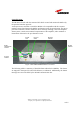
The amplifier is powered from a DC supply voltage, which can range from -36V to -60V.
The DC power is brought into the amplifier through a 3 pins D-Sub connector located on
the front panel of the amplifier. A switch also located on the front panel is to turn on/off
the DC power of amplifier.
A 25-pin D-Sub connector located on the amplifier front panel is used for RS-485
communication. Alarms and operating state are communicated to the outside world
through the RS-485 communications bus, and visible bi-color LED located on the
amplifier front panel.
The RF signal is brought into the amplifier through a pair of female SMA type
connectors located on the front panel of the amplifier. The RF1 input connector is used
by default and the RF2 input is for backup. The amplifier RF signal is brought out of the
amplifier through an N type connector located on the front panel of the amplifier.