
- Analog Devices, Inc. Embedded Processor Specification Sheet

Rev. C | Page 30 of 48 | December 2006
ADSP-TS201S
Link Port Low Voltage, Differential-Signal (LVDS)
Electrical Characteristics, and Timing
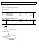
Table 30 and Table 31 with Figure 16 provide the electrical
characteristics for the LVDS link ports. The LVDS link port sig-
nal definitions represent all differential signals with a V
OD
=0V
level and use signal naming without N (negative) and P (posi-
tive) suffixes (see Figure 17).
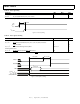
Table 30. Link Port LVDS Transmit Electrical Characteristics
Parameter Description Test Conditions Min Max Unit
V
OH
Output Voltage High, V
O_P
or V
O_N
R
L
= 100 Ω 1.85 V
V
OL
Output Voltage Low, V
O_P
or V
O_N
R
L
= 100 Ω 0.92 V
|V
OD
| Output Differential Voltage R
L
= 100 Ω 300 650 mV
I
OS
Short-Circuit Output Current V
O_P
or V
O_N
= 0 V +5/– 55 mA
V
OD
= 0 V ±10 mA
V
OCM
Common-Mode Output Voltage 1.20 1.50 V
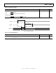
Table 31. Link Port LVDS Receive Electrical Characteristics
Parameter Description Test Conditions Min Max Unit
|V
ID
| Differential Input Voltage t
LDIS
/t
LDIH
≥ 0.20 ns
t
LDIS
/t
LDIH
≥ 0.25 ns
t
LDIS
/t
LDIH
≥ 0.30 ns
t
LDIS
/t
LDIH
≥ 0.35 ns
250
217
206
195
850
850
850
850
mV
mV
mV
mV
V
ICM
Common-Mode Input Voltage 0.6 1.57 V
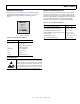
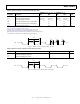
Figure 16. Link Ports—Transmit Electrical Characteristics
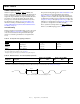
Figure 17. Link Ports—Signals Definition
V
O_N
V
O_P
R
L
V
OCM
=
(V
O_P
+V
O_N
)
2
V
OD
=(V
O_P
–V
O_N
)
Lx<PI N>N
Lx <P IN >P
Lx<PIN>
DIFFERENTI AL PAIR WAVEFORMS
DIFFERENTIAL VO LTAGE WAVEFORM
V
OD
=0V
V
O_N
V
O_P
V
OD
=V
O_P
–V
O_ N