
- Analog Devices, Inc. Embedded Processor Specification Sheet

Rev. C | Page 28 of 48 | December 2006
ADSP-TS201S
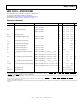
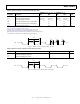
Table 29. AC Signal Specifications
(All values in this table are in nanoseconds.)
Name Description
Input Setup
(Min)
Input Hold
(Min)
Output Valid
(Max)
Output Hold
(Min)
Output Enable
(Min)
1
Output Disable
(Max)
1
Reference
Clock
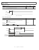
ADDR31–0 External Address Bus 1.5 0.5 4.0 1.0 1.15 2.0 SCLK
DATA63–0 External Data Bus 1.5 0.5 4.0 1.0 1.15 2.0 SCLK
MSH
Memory Select HOST Line — — 4.0 1.0 1.15 2.0 SCLK
MSSD3–0
Memory Select SDRAM Lines 1.5 0.5 4.0 1.0 1.0 2.0 SCLK
MS1–0
Memory Select for Static Blocks — — 4.0 1.0 1.15 2.0 SCLK
RD
Memory Read 1.5 0.5 4.0 1.0 1.15 2.0 SCLK
WRL
Write Low Word 1.5 0.5 4.0 1.0 1.15 2.0 SCLK
WRH
Write High Word 1.5 0.5 4.0 1.0 1.15 2.0 SCLK
ACK Acknowledge for Data High to Low 1.5 0.5 3.6 1.0 1.15 2.0 SCLK
Acknowledge for Data Low to High 1.5 0.5 4.2 0.9 1.15 2.0 SCLK
SDCKE SDRAM Clock Enable 1.5 0.5 4.0 1.0 1.15 2.0 SCLK
RAS
Row Address Select 1.5 0.5 4.0 1.0 1.15 2.0 SCLK
CAS
Column Address Select 1.5 0.5 4.0 1.0 1.15 2.0 SCLK
SDWE
SDRAM Write Enable 1.5 0.5 4.0 1.0 1.15 2.0 SCLK
LDQM Low Word SDRAM Data Mask — — 4.0 1.0 1.15 2.0 SCLK
HDQM High Word SDRAM Data Mask — — 4.0 1.0 1.15 2.0 SCLK
SDA10 SDRAM ADDR10 — — 4.0 1.0 1.15 2.0 SCLK
HBR
Host Bus Request 1.5 0.5 — — — — SCLK
HBG
Host Bus Grant 1.5 0.5 4.0 1.0 1.15 2.0 SCLK
BOFF
Back Off Request 1.5 0.5 — — — — SCLK
BUSLOCK
Bus Lock — — 4.0 1.0 1.15 2.0 SCLK
BRST
Burst Pin 1.5 0.5 4.0 1.0 1.15 2.0 SCLK
BR7–0
Multiprocessing Bus Request Pins 1.5 0.5 4.0 1.0 — — SCLK
BM
Bus Master Debug Aid Only — — 4.0 1.0 — — SCLK
IORD
I/O Read Pin — — 4.0 1.0 1.0 2.0 SCLK
IOWR
I/O Write Pin — — 4.0 1.0 1.15 2.0 SCLK
IOEN
I/O Enable Pin — — 4.0 1.0 1.15 2.0 SCLK
CPA
Core Priority Access High to Low 1.5 0.5 4.0 1.0 0.75 2.0 SCLK
Core Priority Access Low to High 1.5 0.5 29.5 2.0 0.75 2.0 SCLK
DPA
DMA Priority Access High to Low 1.5 0.5 4.0 1.0 0.75 2.0 SCLK
DMA Priority Access Low to High 1.5 0.5 29.5 2.0 0.75 2.0 SCLK
BMS
Boot Memory Select — — 4.0 1.0 1.15 2.0 SCLK
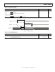
FLAG3–0
2
FLAG Pins — — 4.0 1.0 1.15 2.0 SCLK
RST_IN
3,
4
Global Reset Pin 1.5 2.5 — — — — SCLK
5
TMS Test Mode Select (JTAG) 1.50.5————TCK
TDI Test Data Input (JTAG) 1.50.5————TCK
TDO Test Data Output (JTAG) — — 4.0 1.0 0.75 2.0 TCK
6
TRST
3,
4
Test Reset (JTAG) 1.50.5————TCK
EMU
7
Emulation High to Low — — 5.5 2.0 1.15 4.0 TCK or SCLK
ID2–0
8
Static Pins—Must Be Constant ———————
CONTROLIMP1–0
8
Static Pins—Must Be Constant ———————