
- Analog Devices, Inc. Embedded Processor Specification Sheet

Rev. C | Page 24 of 48 | December 2006
ADSP-TS201S
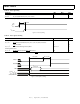
TIMING SPECIFICATIONS
With the exception of DMAR3–0, IRQ3–0, TMR0E, and
FLAG3–0 (input only) pins, all ac timing for the ADSP-TS201S
processor is relative to a reference clock edge. Because input
setup/hold, output valid/hold, and output enable/disable times
are relative to a clock edge, the timing data for the ADSP-
TS201S processor has few calculated (formula-based) values.
For information on ac timing, see General AC Timing. For
information on link port transfer timing, see Link Port Low
Voltage, Differential-Signal (LVDS) Electrical Characteristics,
and Timing on Page 30.
General AC Timing
Timing is measured on signals when they cross the 1.25 V level
as described in Figure 15 on Page 29. All delays (in nanosec-
onds) are measured between the point that the first signal
reaches 1.25 V and the point that the second signal reaches
1.25 V.
The general ac timing data appears in Table 22 and Table 29. All
ac specifications are measured with the load specified in
Figure 36 on Page 38, and with the output drive strength set to
strength 4. In order to calculate the output valid and hold times
for different load conditions and/or output drive strengths, refer
to Figure 37 on Page 38 through Figure 44 on Page 39 (Rise and
Fall Time vs. Load Capacitance) and Figure 45 on Page 39 (Out-
put Valid vs. Load Capacitance and Drive Strength).
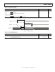
The ac asynchronous timing data for the IRQ3–0
, DMAR3–0,
FLAG3–0, and TMR0E pins appears in Table 21.
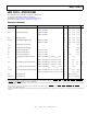
Table 21. AC Asynchronous Signal Specifications
Name Description Pulse Width Low (Min) Pulse Width High (Min)
IRQ3–0
1
Interrupt Request 2 × t
SCLK
ns 2 × t
SCLK
ns
DMAR3–0
1
DMA Request 2 × t
SCLK
ns 2 × t
SCLK
ns
FLAG3–0
2
FLAG3–0 Input 2×t
SCLK
ns 2×t
SCLK
ns
TMR0E
3
Timer 0 Expired 4×t
SCLK
ns —
1
These input pins have Schmitt triggers and therefore do not need to be synchronized to a clock reference.
2
For output specifications on FLAG3–0 pins, see Table 29.
3
This pin is a strap option. During reset, an internal resistor pulls the pin low.
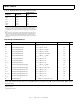
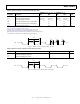
Table 22. Reference Clocks—Core Clock (CCLK) Cycle Time
Parameter Description
Grade = 060 (600 MHz) Grade = 050 (500 MHz)
UnitMin Max Min Max
t
CCLK
1
Core Clock Cycle Time 1.67 12.5 2.0 12.5 ns
1
CCLK is the internal processor clock or instruction cycle time. The period of this clock is equal to the system clock period (t
SCLK
) divided by the system clock ratio
(SCLKRAT2–0). For information on available part numbers for different internal processor clock rates, see the Ordering Guide on Page 46.
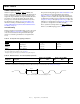
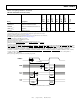
Figure 9. Reference Clocks—Core Clock (CCLK) Cycle Time
CCLK
t
CCLK