
- Analog Devices, Inc. Embedded Processor Specification Sheet

ADSP-TS201S
Rev. C | Page 19 of 48 | December 2006
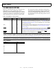
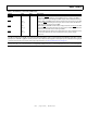
Table 13. Impedance Control Selection
CONTROLIMP1-0 Driver Mode
00 (recommended) Normal
01 Reserved
10 (default) A/D Mode
11 Reserved
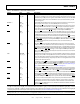
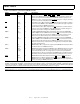
Table 14. Drive Strength/Output Impedance Selection
DS2–0
Pins
Drive
Strength
1
Output
Impedance
2
000 Strength 0 (11.1%) 26 Ω
001 Strength 1 (23.8%) 32 Ω
010 Strength 2 (36.5%) 40 Ω
011 Strength 3 (49.2%) 50 Ω
100 Strength 4 (61.9%) 62 Ω
101 (default) Strength 5 (74.6%) 70 Ω
110 Strength 6 (87.3%) 96 Ω
111 Strength 7 (100%) 120 Ω
1
CONTROLIMP1 = 0, A/D mode disabled.
2
CONTROLIMP1 = 1, A/D mode enabled.
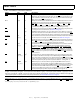
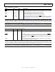
Table 15. Pin Definitions—Power, Ground, and Reference
Signal Type Term Description
V
DD
PnaV
DD
pins for internal logic.
V
DD_A
PnaV
DD
pins for analog circuits. Pay critical attention to bypassing this supply.
V
DD_IO
PnaV
DD
pins for I/O buffers.
V
DD_DRAM
PnaV
DD
pins for internal DRAM.
V
REF
I na Reference voltage defines the trip point for all input buffers, except SCLK, RST_IN,
POR_IN, IRQ3–0, FLAG3–0, DMAR3–0, ID2–0, CONTROLIMP1–0, LxDATO3–0P/N,
LxCLKOUTP/N, LxDATI3–0P/N, LxCLKINP/N, TCK, TDI, TMS, and TRST
. V
REF
can be
connected to a power supply or set by a voltage divider circuit as shown in Figure 6.
For more information, see Filtering Reference Voltage and Clocks on Page 10.
SCLK_V
REF
I na System Clock Reference. Connect this pin to a reference voltage as shown in Figure 7.
For more information, see Filtering Reference Voltage and Clocks on Page 10.
V
SS
GnaGround pins.
NC — nc No Connect. Do not connect these pins to anything (not to any supply, signal, or each
other). These pins are reserved and must be left unconnected.
I = input; A = asynchronous; O = output; OD = open-drain output; T = three-state; P = power supply; G = ground; pd = internal pull-down
5k
Ω; pu = internal pull-up 5 kΩ; pd_0 = internal pull-down 5 kΩ on DSP ID = 0; pu_0 = internal pull-up 5 kΩ on DSP ID = 0; pu_od_0 = internal
pull-up 500
Ω on DSP ID = 0; pd_m = internal pull-down 5 kΩ on DSP bus master; pu_m = internal pull-up 5 kΩ on DSP bus master; pu_ad
= internal pull-up 40 k
Ω. For more pull-down and pull-up information, see Electrical Characteristics on Page 22.
Term (termination of unused pins) column symbols: epd = external pull-down approximately 5 k
Ω to V
SS
; epu = external pull-up approx-
imately 5 k
Ω to V
DD_IO
, nc = not connected; na = not applicable (always used); V
DD_IO
= connect directly to V
DD_IO
; V
SS
= connect directly to V
SS