
- Analog Devices, Inc. Embedded Processor Specification Sheet

ADSP-TS201S
Rev. C | Page 17 of 48 | December 2006
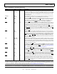
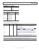
Table 9. Pin Definitions—JTAG Port
Signal Type Term Description
EMU
O/OD nc
1
Emulation. Connected to the DSP’s JTAG emulator target board connector only.
TCK I epd or epu
1
Test Clock (JTAG). Provides an asynchronous clock for JTAG scan.
TDI I (pu_ad) nc
1
Test Data Input (JTAG). A serial data input of the scan path.
TDO O/T nc
1
Test Data Output (JTAG). A serial data output of the scan path.
TMS I (pu_ad) nc
1
Test Mode Select (JTAG). Used to control the test state machine.
TRST
I/A (pu_ad) na Test Reset (JTAG). Resets the test state machine. TRST must be asserted or pulsed low
after power up for proper device operation. For more information, see Reset and
Booting on Page 9.
I = input; A = asynchronous; O = output; OD = open-drain output; T = three-state; P = power supply; G = ground; pd = internal pull-down
5kΩ; pu = internal pull-up 5 kΩ; pd_0 = internal pull-down 5 kΩ on DSP ID = 0; pu_0 = internal pull-up 5 kΩ on DSP ID = 0; pu_od_0 = internal
pull-up 500 Ω on DSP ID = 0; pd_m = internal pull-down 5 kΩ on DSP bus master; pu_m = internal pull-up 5 kΩ on DSP bus master; pu_ad
= internal pull-up 40 k
Ω. For more pull-down and pull-up information, see Electrical Characteristics on Page 22.
Term (termination of unused pins) column symbols: epd = external pull-down approximately 5 k
Ω to V
SS
; epu = external pull-up approx-
imately 5 k
Ω to V
DD_IO
, nc = not connected; na = not applicable (always used); V
DD_IO
= connect directly to V
DD_IO
; V
SS
= connect directly to V
SS
1
See the reference on Page 11 to the JTAG emulation technical reference EE-68.
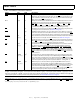
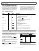
Table 10. Pin Definitions—Flags, Interrupts, and Timer
Signal Type Term Description
FLAG3–0 I/O/A
(pu)
nc FLAG pins. Bidirectional input/output pins can be used as program conditions. Each pin
can be configured individually for input or for output. FLAG3–0 are inputs after power-up
and reset.
IRQ3–0
I/A
(pu)
nc Interrupt Request. When asserted, the DSP generates an interrupt. Each of the IRQ3–0 pins
can be independently set for edge-triggered or level-sensitive operation. After reset, these
pins are disabled unless the IRQ3–0 strap option and interrupt vectors are initialized for
booting.
TMR0E O na Timer 0 expires. This output pulses whenever timer 0 expires. At reset, this is a strap pin.
For more information, see Table 16 on Page 20.
I = input; A = asynchronous; O = output; OD = open-drain output; T = three-state; P = power supply; G = ground; pd = internal pull-down
5k
Ω; pu = internal pull-up 5 kΩ; pd_0 = internal pull-down 5 kΩ on DSP ID = 0; pu_0 = internal pull-up 5 kΩ on DSP ID = 0; pu_od_0 = internal
pull-up 500 Ω on DSP ID = 0; pd_m = internal pull-down 5 kΩ on DSP bus master; pu_m = internal pull-up 5 kΩ on DSP bus master; pu_ad
= internal pull-up 40 k
Ω. For more pull-down and pull-up information, see Electrical Characteristics on Page 22.
Term (termination of unused pins) column symbols: epd = external pull-down approximately 5 k
Ω to V
SS
; epu = external pull-up approx-
imately 5 kΩ to V
DD_IO
, nc = not connected; na = not applicable (always used); V
DD_IO
= connect directly to V
DD_IO
; V
SS
= connect directly to V
SS