
Datasheet


OP97
Rev. F | Page 5 of 16
ABSOLUTE MAXIMUM RATINGS
Absolute maximum ratings apply to both DICE and packaged
parts, unless otherwise noted.
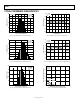
Table 3.
Parameter Rating
Supply Voltage ±20 V
Input Voltage
1
±20 V
Differential Input Voltage
2
±1 V
Differential Input Current
2
±10 mA
Output Short-Circuit Duration Indefinite
Operating Temperature Range
OP97E, OP97F (P, S)
−40°C to +85°C
Storage Temperature Range −65°C to +150°C
Junction Temperature Range −65°C to +150°C
Lead Temperature (Soldering, 60 sec) 300°C
1
For supply voltages less than ±20 V, the absolute maximum input voltage is
equal to the supply voltage.
2
The inputs of the OP97 are protected by back-to-back diodes. Current-
limiting resistors are not used in order to achieve low noise. Differential
input voltages greater than 1 V cause excessive current to flow through the
input protection diodes unless limiting resistance is used.
Stresses above those listed under Absolute Maximum Ratings
may cause permanent damage to the device. This is a stress
rating only; functional operation of the device at these or any
other conditions above those indicated in the operational
section of this specification is not implied. Exposure to absolute
maximum rating conditions for extended periods may affect
device reliability.
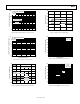
THERMAL RESISTANCE
θ
JA
is specified for the worst-case conditions, that is, a device
soldered in a circuit board for surface-mount packages.
Tab l e 4
.
Package Type θ
JA
1
θ
JC
Unit
8-Lead PDIP (P Suffix) 103 43 °C/W
8-Lead SOIC (S Suffix) 158 43 °C/W
1
θ
JA
is specified for worst-case mounting conditions, that is, θ
JA
is specified for
device in socket for PDIP package; θ
JA
is specified for device soldered to
printed circuit board for SOIC package.
ESD CAUTION