
Datasheet


OP97
Rev. F | Page 4 of 16
V
S
= ±15 V, V
CM
= 0 V, −40°C ≤ T
A
≤ +85°C for the OP97E/OP97F, unless otherwise noted.
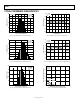
Table 2.
OP97E OP97F
Parameter Symbol Conditions Min Typ Max Min Typ Max Unit
Input Offset Voltage V
OS
25 60 60 200 μV
Average Temperature TCV
OS
S suffix 0.2 0.6 0.3 2.0 μV/°C
Coefficient of V
OS
0.3
Input Offset Current I
OS
60 250 80 750 pA
Average Temperature TCI
OS
0.4 2.5 0.6 7.5 pA/°C
Coefficient of I
OS
Input Bias Current I
B
±60 ±250 ±80 ±750 pA
Average Temperature
Coefficient of I
B
TCI
B
0.4 2.5 0.6 7.5 pA/°C
Large Signal Voltage Gain A
VO
V
O
= 10 V; R
L
= 2 kΩ 200 1000 150 1000 V/mV
Common-Mode Rejection CMR V
CM
= ±13.5 V 108 128 108 128 dB
Power Supply Rejection PSR V
S
= ±2.5 V to ±20 V 108 126 108 128 dB
Input Voltage Range
1
IVR ±13.5 ±14.0 ±13.5 ±14.0 V
Output Voltage Swing V
O
R
L
= 10 kΩ ±13 ±14 ±13 ±14 V
Slew Rate SR 0.05 0.15 0.05 0.15 V/μs
Supply Current I
SY
400 800 400 800 μA
Supply Voltage V
S
Operating range ±2.5 ±15 ±20 ±2.5 ±15 ±20 V
1
Guaranteed by CMR test.