
Datasheet


OP97
Rev. F | Page 3 of 16
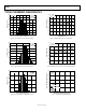
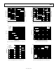
SPECIFICATIONS
ELECTRICAL CHARACTERISTICS
V
S
= ±15 V, V
CM
= 0 V, T
A
= 25°C, unless otherwise noted.
Table 1.
OP97E OP97F
Parameter Symbol Conditions Min Typ Max Min Typ Max Unit
INPUT CHARACTERISTICS
Input Offset Voltage V
OS
10 25 30 75 μV
Long-Term Offset
Voltage Stability ΔV
OS
/Time 0.3 0.3 μV/month
Input Offset Current I
OS
30 100 30 150 pA
Input Bias Current I
B
±30 ±100 ±30 ±150 pA
Input Noise Voltage e
n
p-p 0.1 Hz to 10 Hz 0.5 0.5 μV p-p
Input Noise Voltage Density e
n
f
O
= 10 Hz
1
17 30 17 30 nV/√Hz
f
O
= 1000 Hz
2
14 22 14 22 nV/√Hz
Input Noise Current Density i
n
f
O
= 10 Hz 20 20 fA/√Hz
Large Signal Voltage Gain A
VO
V
O
= ±10 V; R
L
= 2 kΩ 300 2000 200 2000 V/mV
Common-Mode Rejection CMR V
CM
= ±13.5 V 114 132 110 132 dB
Input Voltage Range
3
IVR ±13.5 ±14.0 ±13.5 ±14.0 V
OUTPUT CHARACTERISTICS
Output Voltage Swing V
O
R
L
= 10 kΩ ±13 ±14 ±13 ±14 V
Differential Input Resistance
4
R
IN
30 30 MΩ
POWER SUPPLY
Power Supply Rejection PSR V
S
= ±2 V to ±20 V 114 132 110 132 dB
Supply Current I
SY
380 600 380 600 μA
Supply Voltage V
S
Operating range ±2 ±15 ±20 ±2 ±15 ±20 V
DYNAMIC PERFORMANCE
Slew Rate SR 0.1 0.2 0.1 0.2 V/μs
Closed-Loop Bandwidth BW A
VCL
= 1 0.4 0.9 0.4 0.9 MHz
1
10 Hz noise voltage density is sample tested. Devices 100% tested for noise are available on request.
2
Sample tested.
3
Guaranteed by CMR test.
4
Guaranteed by design.