
Datasheet


DAC8426
–4–
REV. C
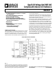
DICE CHARACTERISTICS
DIE SIZE 0.129
×
0.152 inch, 19,608 sq. mils
(3.28
×
3.86 mm, 12.65 sq. mm)
1.
V
OUT B
11. DB
3
2. V
OUT A
12. DB
2
3. V
SS
13. DB
1
4. V
REF
OUT 14. DB
0
(LSB)
5. AGND 15. WR
6. DGND 16. A
1
7. DB
7
(MSB) 17. A
0
8. DB
6
18. V
DD
9. DB
5
19. V
OUT D
10. DB
4
20. V
OUT C
WARNING!
ESD SENSITIVE DEVICE
CAUTION
ESD (electrostatic discharge) sensitive device. Electrostatic charges as high as 4000 V readily
accumulate on the human body and test equipment and can discharge without detection.
Although the DAC8426 features proprietary ESD protection circuitry, permanent damage may
occur on devices subjected to high energy electrostatic discharges. Therefore, proper ESD
precautions are recommended to avoid performance degradation or loss of functionality.
DAC8426GBC
Parameter Symbol Conditions Limits Units
Total Unadjusted Error TUE ±2 LSB max
Relative Accuracy INL ±1 LSB max
Differential Nonlinearity DNL ±1 LSB max
Full-Scale Error G
FSE
±1 LSB max
Zero Code Error V
ZSE
±20 mV max
DAC Output Current I
OUT
SOURCE Digital In = All Ones 10 mA min
Reference Output Voltage V
REF
OUT No Load 10.04 V max
Load Regulation LD
REG
∆I
L
= 5 mA 0.1 %/mA max
Line Regulation LN
REG
∆V
DD
= ±10 V 0.04 %/V max
Reference Output Current I
REF
OUT ∆V
REF
OUT < 40 mV 5 mA min
Logic Inputs High V
INH
2.4 V min
Logic Inputs Low V
INL
0.8 V max
Logic Input Current I
IN
V
IN
= 0 V or V
DD
±1 µA max
Positive Supply Current I
DD
V
IN
= V
INL
or V
INH
14 mA max
Negative Supply Current I
SS
V
IN
= V
INL
or V
INH’
V
SS
= –5 V 10 mA max
NOTE
Electrical tests are performed at wafer probe to the limits shown. Due to variations in assembly methods and normal yield loss, yield after packaging is not guaranteed
for standard product dice. Consult factory to negotiate specifications based on dice lot qualifications through sample lot assembly and testing.
WAFER TEST LIMITS
at V
DD
= +15 V 6 5%; V
SS
= AGND = DGND = 0 V; unless otherwise specified. T
A
= +258C. All specifications
apply for DACs A, B, C, and D.