
Datasheet


ADXL326
Rev. 0 | Page 13 of 16
LAYOUT AND DESIGN RECOMMENDATIONS
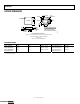
The recommended soldering profile is shown in Figure 25, followed by a description of the profile features in Table 6. The recommended
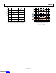
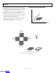
PCB layout or solder land drawing is shown in Figure 26.
t
P
t
L
t25°C TO PEAK
t
S
PREHEAT
CRITICAL ZONE
T
L
TO T
P
TEMPERATURE
TIME
RAMP-DOWN
RAMP-UP
T
SMIN
T
SMAX
T
P
T
L
07948-002
Figure 25. Recommended Soldering Profile
Table 6. Recommended Soldering Profile
Profile Feature Sn63/Pb37 Pb-Free
Average Ramp Rate (T
L
to T
P
) 3°C/sec maximum 3°C/sec maximum
Preheat
Minimum Temperature (T
SMIN
) 100°C 150°C
Maximum Temperature (T
SMAX
) 150°C 200°C
Time (T
SMIN
to T
SMAX
), t
S
60 sec to 120 sec 60 sec to 180 sec
T
SMAX
to T
L
Ramp-Up Rate 3°C/sec maximum 3°C/sec maximum
Time Maintained Above Liquidous (T
L
)
Liquidous Temperature (T
L
) 183°C 217°C
Time (t
L
) 60 sec to 150 sec 60 sec to 150 sec
Peak Temperature (T
P
) 240°C + 0°C/−5°C 260°C + 0°C/−5°C
Time Within 5°C of Actual Peak Temperature (t
P
) 10 sec to 30 sec 20 sec to 40 sec
Ramp-Down Rate 6°C/sec maximum 6°C/sec maximum
Time 25°C to Peak Temperature 6 minutes maximum 8 minutes maximum
C
ENTER PAD IS NOT
INTERNALLY CONNECTED
BUT SHOULD BE SOLDERED
FOR MECHANICAL INTEGRITY
0.50
MAX
0.65 0.325
1.95
0.65
0.325
4
4
0.35
MAX
1.95
DIMENSIONS SHOWN IN MILLIMETERS
07948-004
Figure 26. Recommended PCB Layout
Downloaded from Arrow.com.Downloaded from Arrow.com.Downloaded from Arrow.com.Downloaded from Arrow.com.Downloaded from Arrow.com.Downloaded from Arrow.com.Downloaded from Arrow.com.Downloaded from Arrow.com.Downloaded from Arrow.com.Downloaded from Arrow.com.Downloaded from Arrow.com.Downloaded from Arrow.com.Downloaded from Arrow.com.