
Datasheet


Table Of Contents
- FEATURES
- APPLICATIONS
- FUNCTIONAL BLOCK DIAGRAM
- TABLE OF CONTENTS
- SPECIFICATIONS
- ABSOLUTE MAXIMUM RATINGS
- PIN CONFIGURATION AND FUNCTION DESCRIPTIONS
- GENERAL DESCRIPTION
- TYPICAL PERFORMANCE CHARACTERISTICS
- FEATURES
- COLOR BAR GENERATION
- SQUARE PIXEL MODE
- COLOR SIGNAL CONTROL
- BURST SIGNAL CONTROL
- NTSC PEDESTAL CONTROL
- PIXEL TIMING DESCRIPTION
- SUBCARRIER RESET
- REAL-TIME CONTROL
- Video Timing Description
- Vertical Blanking Data Insertion
- Mode 0 (CCIR-656): Slave Option
- Mode 0 (CCIR-656): Master Option
- Mode 1: Slave Option HSYNC, BLANK, FIELD
- Mode 1: Master Option HSYNC, BLANK, FIELD
- Mode 2: Slave Option HSYNC, VSYNC, BLANK
- Mode 2: Master Option HSYNC, VSYNC, BLANK
- Mode 3: Master/Slave Option HSYNC, BLANK, FIELD
- POWER-ON RESET
- SCH PHASE MODE
- MPU PORT DESCRIPTION
- REGISTER ACCESSES
- REGISTER PROGRAMMING
- SUBADDRESS REGISTER (SR7–SR0)
- REGISTER SELECT (SR5–SR0)
- MODE REGISTER 1 (MR1)
- MODE REGISTER 2 (MR2)
- MODE REGISTER 3 (MR3)
- MODE REGISTER 4 (MR4)
- TIMING MODE REGISTER 0 (TR0)
- TIMING MODE REGISTER 1 (TR1)
- SUBCARRIER FREQUENCY REGISTERS 3–0
- SUBCARRIER PHASE REGISTER
- CLOSED CAPTIONING EVEN FIELD DATA REGISTERS 1–0
- CLOSED CAPTIONING ODD FIELD DATA REGISTERS 1–0
- NTSC PEDESTAL/PAL TELETEXT CONTROL REGISTERS 3–0
- TELETEXT REQUEST CONTROL REGISTER (TC07)
- CGMS_WSS REGISTER 0 (C/W0)
- CGMS_WSS REGISTER 1 (C/W1)
- CGMS_WSS REGISTER 2 (C/W2)
- APPENDIX 1—BOARD DESIGN AND LAYOUT CONSIDERATIONS
- APPENDIX 2—CLOSED CAPTIONING
- APPENDIX 3—COPY GENERATION MANAGEMENT SYSTEM (CGMS)
- APPENDIX 4—WIDE SCREEN SIGNALING (WSS)
- APPENDIX 5—TELETEXT
- APPENDIX 6—WAVEFORMS
- APPENDIX 7—OPTIONAL OUTPUT FILTER
- APPENDIX 8—RECOMMENDED REGISTER VALUES
- OUTLINE DIMENSIONS
ADV7174/ADV7179
Rev. B | Page 42 of 52
APPENDIX 3—COPY GENERATION MANAGEMENT SYSTEM (CGMS)
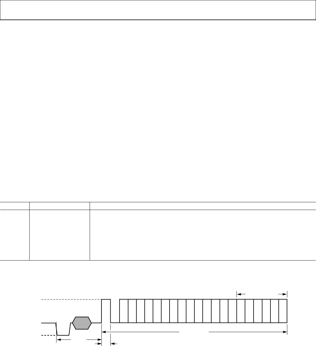
The ADV7174/ADV7179 supports the CGMS, conforming to
the standard. CGMS data is transmitted on Line 20 of the odd
fields and on Line 283 of the even fields. Bits C/W05 and
C/W06 control whether or not CGMS data is output on odd
and even fields. CGMS data can only be transmitted when the
ADV7174/ ADV7179 is configured in NTSC mode. The CGMS
data is 20 bits long, the function of each of these bits is as shown
below. The CGMS data is preceded by a reference pulse of the
same amplitude and duration as a CGMS bit (see Figure 57).
The bits are output from the configuration registers in the
following order: C/W00 = C16, C/W01 = C17, C/W02 = C18,
C/W03 = C19, C/W10 = C8, C/ W11 = C9, C/W12 = C10,
C/W13 = C11, C/W14 = C12, C/ W15 = C13, C/W16 = C14,
C/W17 = C15, C/W20 = C0, C/W21 = C1, C/W22 = C2,
C/W23 = C3, C/W24 = C4, C/W25 = C5, C/W26 = C6, C/W27
= C7. If Bit C/W04 is set to a Logic 1, the last six bits, C19–C14,
which comprise the 6-bit CRC check sequence, are calculated
automatically on the ADV7174/ADV7179 based on the lower
14 bits (C0–C13) of the data in the data registers and output
with the remaining 14 bits to form the complete 20 bits of the
CGMS data. The calculation of the CRC sequence is based on
the polynomial X
6
+ X + 1 with a preset value of 111111. If
C/W04 is set to a Logic 0, all 20 bits (C0–C19) are directly
output from the CGMS registers (no CRC is calculated; it must
be calculated by the user).
FUNCTION OF CGMS BITS
Word 0 –6 Bits
Word 1 –4 Bits
Word 2 –4 Bits
CRC –6 Bits CRC Polynomial = X
6
+ X + 1 (Preset to 111111)
Table 21. Bit 1–Bit 14
Word Bit Function
Word 0 1 0
B1 Aspect Ratio 16:9 4:3
B2 Display Format Letterbox
Normal
B3 Undefined
B4, B5, B6
Identification information about video and other signals, for example, audio
Word 1 B7, B8, B9, B10
Identification signal incidental to Word 0
Word 2 B11, B12, B13, B14 Identification signal and information incidental to Word 0
CRC SEQUENCE
11.2
μ
s
2.235
μ
s ± 20ns
49.1
μ
s ± 0.5
μ
s
REF
C0 C1 C2 C3 C4 C5 C6 C7 C8 C9 C10 C11 C12
C13 C14 C15 C16
C17 C18 C19
100 IRE
70 IRE
0 IRE
–40 IRE
02980-A-056
Figure 57. CGMS Waveform Diagram