
Datasheet


Table Of Contents
- FEATURES
- APPLICATIONS
- FUNCTIONAL BLOCK DIAGRAM
- TABLE OF CONTENTS
- SPECIFICATIONS
- ABSOLUTE MAXIMUM RATINGS
- PIN CONFIGURATION AND FUNCTION DESCRIPTIONS
- GENERAL DESCRIPTION
- TYPICAL PERFORMANCE CHARACTERISTICS
- FEATURES
- COLOR BAR GENERATION
- SQUARE PIXEL MODE
- COLOR SIGNAL CONTROL
- BURST SIGNAL CONTROL
- NTSC PEDESTAL CONTROL
- PIXEL TIMING DESCRIPTION
- SUBCARRIER RESET
- REAL-TIME CONTROL
- Video Timing Description
- Vertical Blanking Data Insertion
- Mode 0 (CCIR-656): Slave Option
- Mode 0 (CCIR-656): Master Option
- Mode 1: Slave Option HSYNC, BLANK, FIELD
- Mode 1: Master Option HSYNC, BLANK, FIELD
- Mode 2: Slave Option HSYNC, VSYNC, BLANK
- Mode 2: Master Option HSYNC, VSYNC, BLANK
- Mode 3: Master/Slave Option HSYNC, BLANK, FIELD
- POWER-ON RESET
- SCH PHASE MODE
- MPU PORT DESCRIPTION
- REGISTER ACCESSES
- REGISTER PROGRAMMING
- SUBADDRESS REGISTER (SR7–SR0)
- REGISTER SELECT (SR5–SR0)
- MODE REGISTER 1 (MR1)
- MODE REGISTER 2 (MR2)
- MODE REGISTER 3 (MR3)
- MODE REGISTER 4 (MR4)
- TIMING MODE REGISTER 0 (TR0)
- TIMING MODE REGISTER 1 (TR1)
- SUBCARRIER FREQUENCY REGISTERS 3–0
- SUBCARRIER PHASE REGISTER
- CLOSED CAPTIONING EVEN FIELD DATA REGISTERS 1–0
- CLOSED CAPTIONING ODD FIELD DATA REGISTERS 1–0
- NTSC PEDESTAL/PAL TELETEXT CONTROL REGISTERS 3–0
- TELETEXT REQUEST CONTROL REGISTER (TC07)
- CGMS_WSS REGISTER 0 (C/W0)
- CGMS_WSS REGISTER 1 (C/W1)
- CGMS_WSS REGISTER 2 (C/W2)
- APPENDIX 1—BOARD DESIGN AND LAYOUT CONSIDERATIONS
- APPENDIX 2—CLOSED CAPTIONING
- APPENDIX 3—COPY GENERATION MANAGEMENT SYSTEM (CGMS)
- APPENDIX 4—WIDE SCREEN SIGNALING (WSS)
- APPENDIX 5—TELETEXT
- APPENDIX 6—WAVEFORMS
- APPENDIX 7—OPTIONAL OUTPUT FILTER
- APPENDIX 8—RECOMMENDED REGISTER VALUES
- OUTLINE DIMENSIONS
ADV7174/ADV7179
Rev. B | Page 34 of 52
TIMING MODE REGISTER 1 (TR1)
Bits: TR17–TR10
Address: SR4–SR0 = 08H
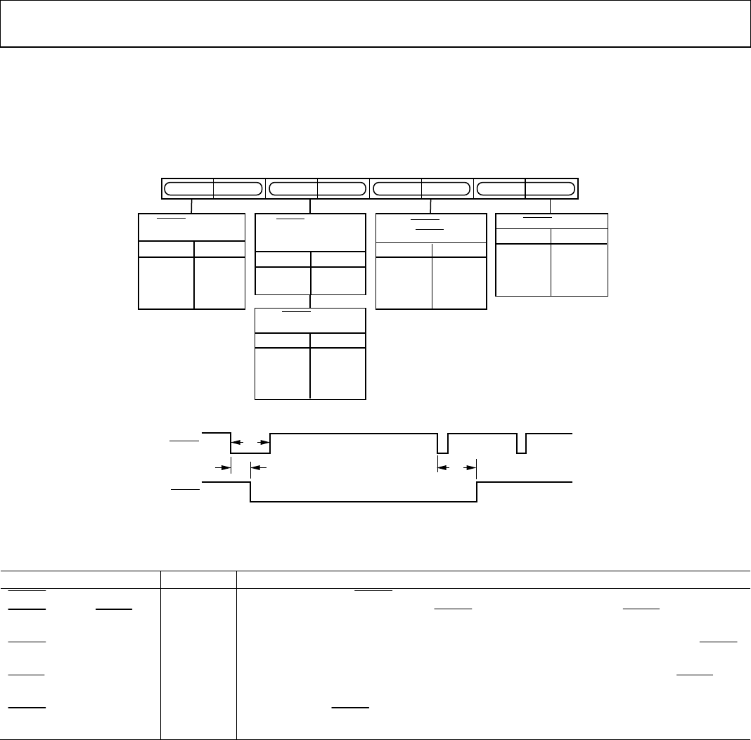
Timing Register 1 is an 8-bit-wide register. Figure 44 shows the various operations under the control of Timing Register 1. This register
can be read from as well written to. This register can be used to adjust the width and position of the master mode timing signals.
TR11 TR10TR17 TR12TR13TR15TR16 TR14
HSYNC TO PIXEL
DATA ADJUST
TR17
TR16
00× T
PCLK
1 × T
PCLK
1 × T
PCLK
4 × T
PCLK
16 × T
PCLK
128 × T
PCLK
0 × T
PCLK
4 × T
PCLK
8 × T
PCLK
16 × T
PCLK
1 × T
PCLK
4 × T
PCLK
16 × T
PCLK
128 × T
PCLK
2 × T
PCLK
3 × T
PCLK
0
1
1
0
1
0
1
HSYNC TO
FIELD/VSYNC DELAY
TR13
TR12
0
0
1
1
0
1
0
1
HSYNC WIDTH
0
0
1
1
0
1
0
1
TR11
TR10
HSYNC TO FIELD
RISING EDGE DELAY
(MODE 1 ONLY)
xT
B
T
B
+ 32μsx
0
1
TR15
TR14
T
C
T
A
T
B
VSYNC WIDTH
(MODE 2 ONLY)
TR15
TR14
0
0
1
1
0
1
0
1
LINE 313 LINE 314LINE 1
TIMING MODE 1 (MASTER/PAL)
HSYNC
FIELD/VSYNC
T
B
T
A
T
C
02980-A-043
Figure 44. Timing Register 1
Table 16. TR1 Bit Description
Bit Name Bit No. Description
These bits adjust the HSYNC
pulse width.
HSYNC
Width
TR11–TR10
These bits adjust the position of the HSYNC
output relative to the FIELD/VSYNC output.
HSYNC
to FIELD/
VSYNC
Delay
TR13–TR12
When the ADV7174/ADV7179 is in Timing Mode 1, these bits adjust the position of the HSYNC
output relative to the FIELD output rising edge.
HSYNC
to FIELD Rising
Edge Delay
TR15–TR14
When the ADV7174/ADV7179 is configured in Timing Mode 2, these bits adjust the VSYNC
pulse width.
VSYNC
Width
TR15–TR14
This enables the HSYNC
to be adjusted with respect to the pixel data. This allows the Cr and Cb
components to be swapped. This adjustment is available in both master and slave timing modes.
HSYNC
to Pixel Data Adjust
TR17–TR16