
Datasheet


Table Of Contents
- FEATURES
- APPLICATIONS
- FUNCTIONAL BLOCK DIAGRAM
- TABLE OF CONTENTS
- SPECIFICATIONS
- ABSOLUTE MAXIMUM RATINGS
- PIN CONFIGURATION AND FUNCTION DESCRIPTIONS
- GENERAL DESCRIPTION
- TYPICAL PERFORMANCE CHARACTERISTICS
- FEATURES
- COLOR BAR GENERATION
- SQUARE PIXEL MODE
- COLOR SIGNAL CONTROL
- BURST SIGNAL CONTROL
- NTSC PEDESTAL CONTROL
- PIXEL TIMING DESCRIPTION
- SUBCARRIER RESET
- REAL-TIME CONTROL
- Video Timing Description
- Vertical Blanking Data Insertion
- Mode 0 (CCIR-656): Slave Option
- Mode 0 (CCIR-656): Master Option
- Mode 1: Slave Option HSYNC, BLANK, FIELD
- Mode 1: Master Option HSYNC, BLANK, FIELD
- Mode 2: Slave Option HSYNC, VSYNC, BLANK
- Mode 2: Master Option HSYNC, VSYNC, BLANK
- Mode 3: Master/Slave Option HSYNC, BLANK, FIELD
- POWER-ON RESET
- SCH PHASE MODE
- MPU PORT DESCRIPTION
- REGISTER ACCESSES
- REGISTER PROGRAMMING
- SUBADDRESS REGISTER (SR7–SR0)
- REGISTER SELECT (SR5–SR0)
- MODE REGISTER 1 (MR1)
- MODE REGISTER 2 (MR2)
- MODE REGISTER 3 (MR3)
- MODE REGISTER 4 (MR4)
- TIMING MODE REGISTER 0 (TR0)
- TIMING MODE REGISTER 1 (TR1)
- SUBCARRIER FREQUENCY REGISTERS 3–0
- SUBCARRIER PHASE REGISTER
- CLOSED CAPTIONING EVEN FIELD DATA REGISTERS 1–0
- CLOSED CAPTIONING ODD FIELD DATA REGISTERS 1–0
- NTSC PEDESTAL/PAL TELETEXT CONTROL REGISTERS 3–0
- TELETEXT REQUEST CONTROL REGISTER (TC07)
- CGMS_WSS REGISTER 0 (C/W0)
- CGMS_WSS REGISTER 1 (C/W1)
- CGMS_WSS REGISTER 2 (C/W2)
- APPENDIX 1—BOARD DESIGN AND LAYOUT CONSIDERATIONS
- APPENDIX 2—CLOSED CAPTIONING
- APPENDIX 3—COPY GENERATION MANAGEMENT SYSTEM (CGMS)
- APPENDIX 4—WIDE SCREEN SIGNALING (WSS)
- APPENDIX 5—TELETEXT
- APPENDIX 6—WAVEFORMS
- APPENDIX 7—OPTIONAL OUTPUT FILTER
- APPENDIX 8—RECOMMENDED REGISTER VALUES
- OUTLINE DIMENSIONS
ADV7174/ADV7179
Rev. B | Page 33 of 52
TIMING MODE REGISTER 0 (TR0)
Bits: TR07–TR00
Address: SR4–SR0 = 07H
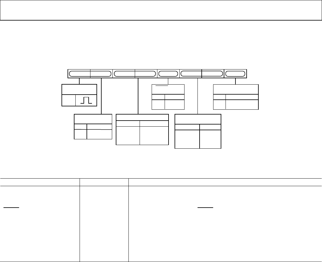
Figure 43 shows the various operations under the control of Timing Register 0. This register can be read from as well as written to.
TR01
TR00TR07
TR02TR03TR05TR06 TR04
TIMING
REGISTER RESET
TR07
BLANK INPUT
CONTROL
0 ENABLE
1 DISABLE
TR03
PIXEL PORT
CONTROL
0 8 BIT
1 FORBIDDEN
TR06
MASTER/SLAVE
CONTROL
0 SLAVE TIMING
1 MASTER TIMING
TR00
LUMA DELAY
0 0ns DELAY
0 74ns DELAY
1 148ns DELAY
1
0
1
0
1 222ns DELAY
TR05
TR04
TIMING MODE
SELECTION
0 MODE 0
0 MODE 1
1 MODE 2
1
0
1
0
1 MODE 3
TR02
TR01
02980-A-042
Figure 43. Timing Register 0
Table 15. TR0 Bit Description
Bit Name Bit No. Description
Master/Slave Control TR00 This bit controls whether the ADV7174/ADV7179 is in master or slave mode.
Timing Mode Selection TR02–TR01
These bits control the timing mode of the ADV7174/ADV7179. These modes are
described in more detail in the 3.3 V Timing Specifications table.
BLANK
Input Control
TR03
This bit controls whether the BLANK input is used when the part is in slave mode.
Luma Delay TR05–TR04
These bits control the addition of a luminance delay. Each bit represents a delay of
74 ns.
Pixel Port Control TR06
This bit is used to set the pixel port to accept 8-bit or YCrCb data on Pins P7–P0.
0 must be written here.
Timing Register Reset TR07
Toggling the TR07 from low to high and to low again resets the internal timing
counters. This bit should be toggled after power-up, reset, or changing to a new
timing mode.