
Datasheet


ADV3221/ADV3222
Rev. 0 | Page 7 of 20
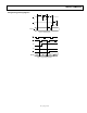
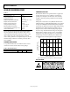
PIN CONFIGURATION AND FUNCTION DESCRIPTIONS
IN0
1
GND 2
IN1
3
GND 4
V+
16
A015
A1
14
CS13
IN2 5 OUT12
GND
6
CK2
11
IN3 7 CK110
GND 8 V–9
ADV3221/
ADV3222
TOP VIEW
(Not to Scale)
08652-005
Figure 5. Pin Configuration
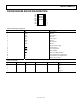
Table 6. Pin Function Descriptions
Pin No. Mnemonic Description
1 IN0 Analog Input
2 GND Ground
3 IN1 Analog Input
4 GND Ground
5 IN2 Analog Input
6 GND Ground
7 IN3 Analog Input
8 GND Ground
9 V− Negative Power Supply
10
CK1
First Rank Clock
11
CK2
Second Rank Clock
12 OUT Analog Output
13
CS
Chip Select (Output Enable)
14 A1 Select Address Most Significant Bit
15 A0 Select Address Least Significant Bit
16 V+ Positive Power Supply
Table 7. Truth Table
CS
A1 A0
CK1
CK2
Output
0 0 0 0 0 IN0
0 0 1 0 0 IN1
0 1 0 0 0 IN2
0 1 1 0 0 IN3
1 X
1
X
1
0 0 High-Z
1
X is don’t care.