
Datasheet


ADV3221/ADV3222
Rev. 0 | Page 4 of 20
ADV3221 ADV3222
Parameter Test Conditions/Comments Min Typ Max Min Typ Max Unit
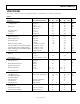
POWER SUPPLIES
Supply Current V+, output enabled, no load 7 8 7.5 9 mA
V+, output disabled (
CS
high)
1.6 2.0 1.8 2.2 mA
V−, output enabled, no load 7 8 7.5 9 mA
V−, output disabled (
CS
high)
1.6 2.0 1.8 2.2 mA
Supply Voltage Range ±4.5 ±5.5 ±4.5 ±5.5 V
Power Supply Rejection (PSR) f = 100 kHz −70 −65 dB
f = 1 MHz −60 −55 dB
TEMPERATURE
Operating Temperature Range Still air −40 +85 −40 +85 °C
Junction-to-Ambient Thermal Impedance (θ
JA
) Operating (still air) 81 81 °C/W
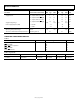
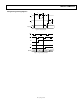
TIMING AND LOGIC CHARACTERISTICS
Table 2.
Parameter Symbol Min Typ Max Unit
A0, A1,
CS
Setup Time
t
1
20 ns
CK1
Pulse Width
t
2
40 ns
CK1
to
CK2
Pulse Separation
t
3
40 ns
CK2
Pulse Width
t
4
40 ns
A0, A1,
CS
Hold Time
t
5
20 ns
Table 3. Logic Levels
V
IH
V
IL
I
IH
I
IL
I
IH
I
IL
A0, A1,
CK1
,
CK2
,
CS
A0, A1,
CK1
,
CK2
,
CS
A0, A1,
CS
A0, A1,
CS
CK1
,
CK2
CK1
,
CK2
+2.0 V min +0.8 V max ±2 μA max ±2 μA max +60 μA max +10 μA max