
Datasheet
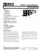


800 MHz, 4:1 Analog Multiplexer
ADV3221/ADV3222
Rev. 0
Information furnished by Analog Devices is believed to be accurate and reliable. However, no
responsibility is assumed by Analog Devices for its use, nor for any infringements of patents or other
rights of third parties that may result from its use. Specifications subject to change without notice. No
license is granted by implication or otherwise under any patent or patent rights of Analog Devices.
Trademarks and registered trademarks are the property of their respective owners.
One Technology Way, P.O. Box 9106, Norwood, MA 02062-9106, U.S.A.
Tel: 781.329.4700 www.analog.com
Fax: 781.461.3113 ©2010 Analog Devices, Inc. All rights reserved.
FEATURES
Excellent ac performance
−3 dB bandwidth
800 MHz (200 mV p-p)
750 MHz (2 V p-p)
Slew rate: 2400 V/μs
Low power: 75 mW, V
S
= ±5 V
Excellent video performance
100 MHz, 0.1 dB gain flatness
0.02% differential gain error/0.02° differential phase error
(R
L
= 150 Ω)
ADV3221 is a pin-for-pin upgrade to the HA4344
Gain = +1 (ADV3221) or gain = +2 (ADV3222)
Low all hostile crosstalk of −85 dB @ 5 MHz, and
−58 dB @ 100 MHz
Latched control lines for synchronous switching
High impedance output disable allows connection of
multiple devices without loading the output bus
16-lead SOIC
APPLICATIONS
Routing of high speed signals including
Video (NTSC, PAL, S, SECAM, YUV, RGB)
Compressed video (MPEG, wavelet)
3-level digital video (HDB3)
Data communications
Telecommunications
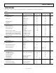
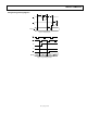
FUNCTIONAL BLOCK DIAGRAM
DQ
LATCH
DQ
LATCH
DQ
LATCH
DQ
LATCH
DQ
LATCH
DQ
LATCH
DECODE
100kΩ 100kΩ
A0
A1
C
K1
C
K2
CS
IN0
IN1
IN2
IN3
G = +1
(G = +2)
OUT
ENABLE
08652-001
Figure 1.
GENERAL DESCRIPTION
The ADV3221 and ADV3222 are high speed, high slew rate,
buffered 4:1 analog multiplexers. They offer a −3 dB signal
bandwidth greater than 800 MHz and channel switch times
of less than 20 ns with 1% settling. With lower than −58 dB of
crosstalk and −67 dB isolation (at 100 MHz), the ADV3221 and
ADV3222 are useful in many high speed applications. The diffe-
rential gain error of less than 0.02% and differential phase error
of less than 0.02°, together with 0.1 dB gain flatness out to 100 MHz
while driving a 75 Ω back terminated load, make the ADV3221
and ADV3222 ideal for all types of signal switching.
The ADV3221/ADV3222 include an output buffer that can be
placed into a high impedance state. This allows multiple outputs
to be connected together for cascading stages without the off
channels loading the output bus. The ADV3221 has a gain of
+1, and the ADV3222 has a gain of +2; they both operate on ±5 V
supplies while consuming less than 7.5 mA of idle current. The
channel switching is performed via latched control lines, allowing
synchronous updating in a multiple ADV3221/ADV3222 envi-
ronment.
The ADV3221/ADV3222 are offered in a 16-lead SOIC package
and are available over the extended industrial temperature range of
−40°C to +85°C.