
Inc. Computer Hardware User Manual

REV. B
ADuC812
–7–
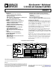
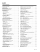
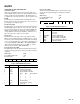
PIN FUNCTION DESCRIPTIONS
Mnemonic Type Function
DV
DD
P Digital Positive Supply Voltage, 3 V or 5 V Nominal
AV
DD
P Analog Positive Supply Voltage, 3 V or 5 V Nominal
C
REF
I Decoupling Input for On-Chip Reference. Connect 0.1 µF between this pin and AGND.
V
REF
I/O Reference Input/Output. This pin is connected to the internal reference through a series resistor and is the
reference source for the analog-to-digital converter. The nominal internal reference voltage is 2.5 V and this
appears at the pin. This pin can be overdriven by an external reference.
AGND G Analog Ground. Ground Reference point for the analog circuitry.
P1.0–P1.7 I Port 1 is an 8-bit Input Port only. Unlike other Ports, Port 1 defaults to Analog Input Mode, to configure
any of these Port Pins as a digital input, write a “0” to the port bit. Port 1 pins are multifunction and share
the following functionality.
ADC0–ADC7 I Analog Inputs. Eight single-ended analog inputs. Channel selection is via ADCCON2 SFR.
T2 I Timer 2 Digital Input. Input to Timer/Counter 2. When Enabled, Counter 2 is incremented in response to
a 1 to 0 transition of the T2 input.
T2EX I Digital Input. Capture/Reload trigger for Counter 2 and also functions as an Up/Down control input for
Counter 2.
SS I Slave Select Input for the SPI Interface
SDATA I/O User Selectable, I
2
C-Compatible or SPI Data Input/Output Pin
SCLOCK I/O Serial Clock Pin for I
2
C-Compatible or SPI Serial Interface Clock
MOSI I/O SPI Master Output/Slave Input Data I/O Pin for SPI Interface
MISO I/O SPI Master Input/Slave Output Data I/O Pin for SPI Serial Interface
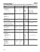
DAC0 O Voltage Output from DAC0
DAC1 O Voltage Output from DAC1
RESET I Digital Input. A high level on this pin for 24 master clock cycles while the oscillator is running resets the
device. External power-on reset (POR) circuity must be implemented to drive the RESET pin as described
in the Power-On Reset Operation section of this data sheet.
P3.0–P3.7 I/O Port 3 is a bidirectional port with internal pull-up resistors. Port 3 pins that have 1s written to them are
pulled high by the internal pull-up resistors, and in that state they can be used as inputs. As inputs Port 3
pins being pulled externally low will source current because of the internal pull-up resistors. Port 3 pins also
contain various secondary functions which are described below.
RxD I/O Receiver Data Input (Asynchronous) or Data Input/Output (Synchronous) of Serial (UART) Port
TxD O Transmitter Data Output (Asynchronous) or Clock Output (Synchronous) of Serial (UART) Port
INT0 I Interrupt 0, programmable edge or level triggered Interrupt input, which can be programmed to one of two
priority levels. This pin can also be used as a gate control input to Timer 0.
INT1 I Interrupt 1, programmable edge or level triggered Interrupt input, which can be programmed to one of two
priority levels. This pin can also be used as a gate control input to Timer 1.
T0 I Timer/Counter 0 Input
T1 I Timer/Counter 1 Input
CONVST I Active low Convert Start Logic input for the ADC block when the external Convert start function is enabled.
A low-to-high transition on this input puts the track/hold into its hold mode and starts conversion.
WR O Write Control Signal, Logic Output. Latches the data byte from Port 0 into the external data memory.
RD O Read Control Signal, Logic Output. Enables the external data memory to Port 0.
XTAL2 O Output of the Inverting Oscillator Amplifier
XTAL1 I Input to the inverting oscillator amplifier and input to the internal clock generator circuits.
DGND G Digital Ground. Ground reference point for the digital circuitry.
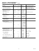
P2.0–P2.7 I/O Port 2 is a bidirectional port with internal pull-up resistors. Port 2 pins that have 1s written to them are
(A8–A15) pulled high by the internal pull-up resistors, and in that state they can be used as inputs. As inputs Port 2
(A16–A23) pins being pulled externally low will source current because of the internal pull-up resistors. Port 2 emits
the high order address bytes during fetches from external program memory and middle and high order
address bytes during accesses to the external 24-bit external data memory space.