
Inc. Computer Hardware User Manual

REV. B
ADuC812
–21–
USER INTERFACE TO OTHER ON-CHIP ADuC812
PERIPHERALS
The following section gives a brief overview of the various
peripherals also available on-chip. A summary of the SFRs used to
control and configure these peripherals is also given.
DAC
The ADuC812 incorporates two 12-bit, voltage output DACs
on-chip. Each has a rail-to-rail voltage output buffer capable
of driving 10 kΩ/100 pF. Each has two selectable ranges, 0 V to
V
REF
(the internal bandgap 2.5 V reference) and 0 V to AV
DD
.
Each can operate in 12-bit or 8-bit mode. Both DACs share a
control
register, DACCON, and four data registers, DAC1H/L,
DAC0H/L.
It should be noted that in 12-bit asynchronous mode,
the DAC voltage output will be updated as soon as the DACL
data SFR has been written; therefore, the DAC data registers
should be updated as DACH first, followed by DACL.
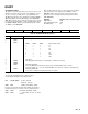
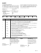
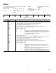
DACCON DAC Control Register
SFR Address FDH
Power-On Default Value 04H
Bit Addressable No
EDOM1GNR0GNR1RLC0RLCCNYS1DP0DP
Table VIII. DACCON SFR Bit Designations
Bit Name Description
7 MODE The DAC MODE bit sets the overriding operating mode for both DACs.
Set to “1” = 8-Bit Mode (Write 8 Bits to DACxL SFR).
Set to “0”= 12-Bit Mode.
6 RNG1 DAC1 Range Select Bit.
Set to “1” = DAC1 Range 0–V
DD
.
Set to “0” = DAC1 Range 0–V
REF
.
5 RNG0 DAC0 Range Select Bit.
Set to “1” = DAC0 Range 0–V
DD.
Set to “0” = DAC0 Range 0–V
REF.
4 CLR1 DAC1 Clear Bit.
Set to “0” = DAC1 Output Forced to 0 V.
Set to “1” = DAC1 Output Normal.
3 CLR0 DAC0 Clear Bit.
Set to “0” = DAC1 Output Forced to 0 V.
Set to “1” = DAC1 Output Normal.
2 SYNC DAC0/1 Update Synchronization Bit.
When set to “1” the DAC outputs update as soon as DACxL SFRs are written. The user can
simultaneously update both DACs by first updating the DACxL/H SFRs while SYNC is “0.” Both
DACs will then update simultaneously when the SYNC bit is set to “1.”
1 PD1 DAC1 Power-Down Bit.
Set to “1” = Power-On DAC1.
Set to “0” = Power-Off DAC1.
0 PD0 DAC0 Power-Down Bit.
Set to “1” = Power-On DAC0.
Set to “0” = Power-Off DAC0.
DACxH/L DAC Data Registers
Function DAC Data Registers, written by user to update the DAC output.
SFR Address DAC0L (DAC0 Data Low Byte) –>F9H; DAC1L (DAC1 Data Low Byte)->FBH
DAC0H (DAC0 Data High Byte) –>FAH; DAC1H(DAC1 Data High Byte)->FCH
Power-On Default Value 00H –>All four Registers
Bit Addressable No –>All four Registers
The 12-bit DAC data should be written into DACxH/L right-justified such that DACL contains the lower eight bits, and the lower
nibble of DACH contains the upper four bits.