
Inc. Computer Hardware User Manual

REV. B
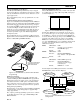
ADuC812
–13–
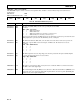
ADCCON1 – (ADC Control SFR #1)
The ADCCON1 register controls conversion and acquisition times, hardware conversion modes and power-down modes as
detailed below.
SFR Address: EFH
SFR Power-On Default Value: 20H
Table III. ADCCON1 SFR Bit Designations
Bit Name Description
ADCCON1.7 MD1 The mode bits (MD1, MD0) select the active operating mode of the ADC
ADCCON1.6 MD0 as follows:
MD1 MD0 Active Mode
0 0 ADC powered down.
0 1 ADC normal mode
1 0 ADC powered down if not executing a conversion cycle.
1 1 ADC standby if not executing a conversion cycle.
Note: In powered down mode the ADC V
REF
circuits are maintained on, whereas in power-down mode all
ADC peripherals are powered down thus minimizing current consumption.
ADCCON1.5 CK1 The ADC clock divide bits (CK1, CK0) select the divide ratio for the master clock used to generate the
ADCCON1.4 CK0 ADC clock. A typical ADC conversion will require 17 ADC clocks. The divider ratio is selected
as follows:
CK1 CK0 MCLK Divider
001
012
104
118
ADCCON1.3 AQ1 The ADC acquisition select bits (AQ1, AQ0) select the time provided for the input track/hold amplifier
ADCCON1.2 AQ0 to acquire the input signal and are selected as follows:
AQ1 AQ0 #ADC Clks
001
012
104
118
ADCCON1.1 T2C The Timer 2 conversion bit (T2C) is set by the user to enable the Timer 2 over flow bit be used as
the ADC convert start trigger input.
ADCCON1.0 EXC The external trigger enable bit (EXC) is set by the user to allow the external Pin 23 (CONVST) to be
used as the active low convert start input. This input should be an active low pulse (minimum pulse
width >100 ns) at the required sample rate.
1DM0DM1KC0KC1QA0QAC2TCXE