
2/40-Bit IEEE Floating-Point DSP Microprocessor Specification Sheet

ADSP-21020
REV. C
–20–
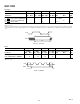
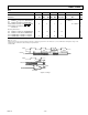
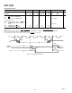
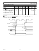
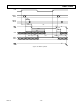
Memory Write
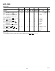
K/B/T Grade K/B/T Grade B/T Grade K Grade
20 MHz 25 MHz 30 MHz 33.3 MHz Frequency Dependency*
Parameter Min Max Min Max Min Max Min Max Min Max Unit
Timing Requirement: 12
t
DAAK
xACK Delay from Address, Select 27 18 6 9 27 + 7DT/8 ns
t
DWAK
xACK Delay from xWR Low 15 10 10 5 15 + DT/2 ns
t
SAK
xACK Setup before CLKIN High 14 12 0 9 14 + DT/4 ns
t
HAK
xACK Hold after CLKIN High 0 0 0 ns
Switching Characteristic:
t
DAWH
Address, Select to xWR Deasserted 37 28 21 18 37+ 15DT/16 ns
t
DAWL
Address, Select to xWR Low 11 7 5 3 11 + 3DT/8 ns
t
WW
xWR Pulse Width 26 20 16 15 26 + 9DT/16 ns
t
DDWH
Data Setup before xWR High 23 18 14 13 23 + DT/2 ns
t
DWHA
Address, Select Hold after xWR
Deasserted 1 0 0 0 1 + DT/16 ns
t
HDWH
Data Hold after xWR Deasserted
1
0 –1 –1 –1 DT/16 ns
t
DAP
xPAGE Delay from Address, Select 1 1 1 1 ns
t
DCKWL
CLKIN High to xWR Low 16 26 13 24 12 22 11 21 16 + DT/4 26 + DT/4 ns
t
WWR
xWR High to xWR or xRD Low 17 13 10 8 17 + 7DT/16 ns
t
DDWR
Data Disable before xWR or xRD
Low 13 9 7 5 13 + 3DT/8 ns
t
WDE
xWR Low to Data Enabled 0 –1 –1 –1 DT/16 ns
NOTES
*DT = t
C
– 50 ns
See “System Hold Time Calculation” in “Test Conditions” section for calculating hold times given capacitive and DC loads.
x = PM or DM; Address = PMA23-0, DMA31-0; Data = PMD47-0, DMD39-0; Select = PMS1-0, DMS3-0.