
Datasheet


3 V LVDS Quad CMOS
Differential Line Receiver
ADN4668
Rev. A
Information furnished by Analog Devices is believed to be accurate and reliable. However, no
responsibility is assumed by Analog Devices for its use, nor for any infringements of patents or other
rights of third parties that may result from its use. Specifications subject to change without notice. No
license is granted by implication or otherwise under any patent or patent rights of Analog Devices.
Trademarks and registered trademarks are the property of their respective owners.
One Technology Way, P.O. Box 9106, Norwood, MA 02062-9106, U.S.A.
Tel: 781.329.4700 www.analog.com
Fax: 781.461.3113 ©2008 Analog Devices, Inc. All rights reserved.
FEATURES
±15 kV ESD protection on receiver input pins
400 Mbps (200 MHz) switching rates
Flow-through pin configuration simplifies PCB layout
150 ps channel-to-channel skew (typical)
100 ps differential skew (typical)
2.7 ns maximum propagation delay
3.3 V power supply
High impedance outputs on power-down
Low power design (3 mW quiescent typical)
Interoperable with existing 5 V LVDS drivers
Accepts small swing (310 mV typical) differential
input signal levels
Supports open, short, and terminated input fail-safe
0 V to −100 mV threshold region
Conforms to TIA/EIA-644 LVDS standard
Industrial operating temperature range of −40°C to +85°C
Available in 16-lead surface-mount SOIC and 16-lead low
profile TSSOP package
APPLICATIONS
Point-to-point data transmission
Multidrop buses
Clock distribution networks
Backplane receivers
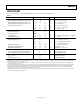
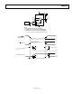
FUNCTIONAL BLOCK DIAGRAM
R1
R2
R3
R4
R
IN1+
V
CC
GND
ADN4668
R
IN1–
R
IN2+
R
IN2–
R
IN3+
R
IN3–
R
IN4+
R
OUT1
R
OUT2
R
OUT3
R
OUT4
R
IN4–
EN
EN
07237-001
Figure 1.
GENERAL DESCRIPTION
The ADN4668 is a quad-channel CMOS, low voltage differential
signaling (LVDS) line receiver offering data rates of over 400 Mbps
(200 MHz) and ultralow power consumption. It features a flow-
through pin configuration for easy PCB layout and separation
of input and output signals.
The device accepts low voltage (310 mV typical) differential
input signals and converts them to a single-ended, 3 V TTL/CMOS
logic level.
The ADN4668 also offers active-high and active-low enable/disable
inputs (EN and
EN
) that control all four receivers. They disable
the receivers and switch the outputs to a high impedance state.
This high impedance state allows the outputs of one or more
ADN4668s to be multiplexed together and reduces the quies-
cent power consumption to 3 mW typical.
The ADN4668 and its companion driver, the ADN4667, offer
a new solution to high speed, point-to-point data transmission
and a low power alternative to emitter-coupled logic (ECL) or
positive emitter-coupled logic (PECL).