
Datasheet


ADG741/ADG742
Rev. A | Page 8 of 12
TERMINOLOGY
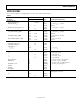
R
ON
Ohmic resistance between D and S.
R
FLAT (ON)
Flatness is defined as the difference between the maximum and
minimum value of on resistance as measured.
I
S
(OFF)
Source leakage current with the switch off.
I
D
(OFF)
Drain leakage current with the switch off.
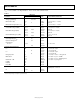
I
D
, I
S
(ON)
Channel leakage current with the switch on.
V
D
(V
S
)
Analog voltage on Terminal D and Terminal S.
C
S
(OFF)
Off switch source capacitance. Measured with reference to
ground.
C
D
(OFF)
Off switch drain capacitance. Measured with reference to
ground.
C
D
, C
S
(ON)
On switch capacitance. Measured with reference to ground.
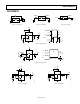
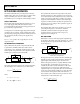
t
ON
Delay time between the 50% and the 90% points of the digital
input and switch on condition. See Figure 14.
t
OFF
Delay time between the 50% and the 90% points of the digital
input and switch off condition.
Off Isolation
A measure of unwanted signal coupling through an off switch.
Charge Injection
A measure of the glitch impulse transferred from the digital
input to the analog output during on-off switching.
Bandwidth
The frequency at which the output is attenuated by −3 dB.
On Response
The frequency response of the on switch.
On Loss
The voltage drop across the on switch as how many dBs the
signal is away from 0 dB at very low frequencies. See Figure 10.