
Datasheet


ADG526A/ADG527A
Rev. C | Page 9 of 20
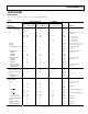
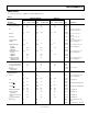
DA
V
SS
S8A
S7A
S6A
S5A
S4A
S3A
S2A
S1A
EN
A0
A1
A2
V
DD
DB
S8B
S7B
S6B
S5B
S4B
S3B
S2B
S1B
GND
NC
RS
WR
1
2
3
4
28
27
26
25
5
6
7
24
23
22
8 21
9 20
10 19
11 18
12 17
13 16
14 15
NC = NO CONNECT
ADG527A
TOP VIEW
(Not to Scale)
01532-006
Figure 5. ADG527A PDIP, SOIC Pin Configuration
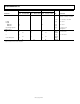
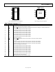
1282726234
5
6
7
8
9
10
11
25
24
23
22
21
20
19
NC = NO CONNECT
S7B
S6B
S5B
S4B
S3B
S2B
S1B
S7A
S6A
S5A
S4A
S3A
S2A
S1A
S8B
RS
DB
V
DD
DA
V
SS
S8A
GND
WR
NC
A2
A1
A0
EN
PIN 1
IDENTFIER
12 13 14 15 16 17 18
ADG527A
TOP VIEW
(Not to Scale)
01532-008
Figure 6. ADG527A PLCC Pin Configuration
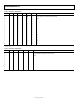
Table 5. ADG527A Pin Function Descriptions
Pin No. Mnemonic Description
1 V
DD
Most Positive Power Supply Potential.
2 DB Drain Terminal. This pin can be an input or output.
3
RS
Reset. The RS signal clears both the address and enable data in the latches resulting in no output (all switches off).
4 S8B Source Terminal. This pin can be an input or output.
5 S7B Source Terminal. This pin can be an input or output.
6 S6B Source Terminal. This pin can be an input or output.
7 S5B Source Terminal. This pin can be an input or output.
8 S4B Source Terminal. This pin can be an input or output.
9 S3B Source Terminal. This pin can be an input or output.
10 S2B Source Terminal. This pin can be an input or output.
11 S1B Source Terminal. This pin can be an input or output.
12 GND Ground (0 V) Reference.
13
WR
Write. The WR signal latches the state of the address control lines and the enable line.
14 NC No Connect.
15 A2 Logic Control Inputs. Selects which source terminal is connected to the drain (D).
16 A1 Logic Control Inputs. Selects which source terminal is connected to the drain (D).
17 A0 Logic Control Inputs. Selects which source terminal is connected to the drain (D).
18 EN Enable. Active high logic control input.
19 S1A Source Terminal. This pin can be an input or output.
20 S2A Source Terminal. This pin can be an input or output.
21 S3A Source Terminal. This pin can be an input or output.
22 S4A Source Terminal. This pin can be an input or output.
23 S5A Source Terminal. This pin can be an input or output.
24 S6A Source Terminal. This pin can be an input or output.
25 S7A Source Terminal. This pin can be an input or output.
26 S8A Source Terminal. This pin can be an input or output.
27 V
SS
Most Negative Power Supply Potential.
28 DA Drain Terminal. This pin can be an input or output.