
Datasheet


ADG526A/ADG527A
Rev. C | Page 7 of 20
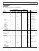
ABSOLUTE MAXIMUM RATINGS
T
A
= 25°C, unless otherwise noted.
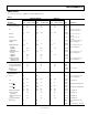
Table 3.
Parameter Rating
V
DD
to V
SS
44 V
V
DD
to GND 25 V
V
SS
to GND
−25 V
Analog Inputs
1
Voltage at Sx or Dx Pins
V
SS
− 2 V to V
DD
+ 2 V
or 20 mA, whichever
occurs first
Continuous Current, Sx or Dx Pins 20 mA
Pulsed Current, Sx or Dx Pins
1 ms Duration, 10% Duty Cycle 40 mA
Digital Inputs
1
Voltage at A, EN, WR, RS
V
SS
− 4 V to V
DD
+ 4 V
or 20 mA, whichever
occurs first
Power Dissipation (Any Package)
Up to 75°C 470 mW
Derates Above 75°C 6 mW/°C
Operating Temperature Range
Commercial (K Version)
−40°C to +85°C
Industrial (B Version)
−40°C to +85°C
Storage Temperature Range
−65°C to +150°C
Lead Temperature (Soldering, 10 sec) 300°C
1
Overvoltage at A, EN,
WR
,
RS
, Sx, or Dx pins are clamped by diodes. Limit
current to the maximum rating in . Table 3
Stresses above those listed under Absolute Maximum Ratings
may cause permanent damage to the device. This is a stress
rating only; functional operation of the device at these or any
other conditions above those indicated in the operational
section of this specification is not implied. Exposure to absolute
maximum rating conditions for extended periods may affect
device reliability.
ESD CAUTION