
Datasheet


ADG526A/ADG527A
Rev. C | Page 13 of 20
TIMING
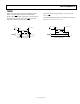
Figure 13 shows the timing sequence for latching the switch
address and enable inputs. The latches are level sensitive;
therefore, while
WR
is held low, the latches are transparent and
the switches respond to the address and enable inputs. This
input data is latched on the rising edge of
WR
.
3
V
0V
3V
0V
WR
EN, A0, A1,
A2, (A3)
1.5V
2.0V
0.8V
t
W
t
S
t
H
01532-003
Figure 13. Timing Sequence
Figure 14 shows the reset pulse width, t
RS
, and reset turn-off
time, t
OFF
(
RS
).
Note that all digital input signal rise and fall times are measured
from 10% to 90% of 3 V, t
R
= t
F
= 20 ns.
t
RS
t
OFF
(RS)
3
V
0V
V
O
0V
RS
0.8V
1.5V
SWITCH
O
UTPUT
01532-004
Figure 14. Reset Pulse