
Datasheet


ADG5233/ADG5234 Data Sheet
Rev. B | Page 10 of 24
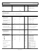
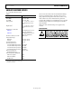
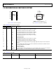
PIN CONFIGURATIONS AND FUNCTION DESCRIPTIONS
Figure 3. ADG5233 TSSOP Pin Configuration Figure 4. ADG5233 LFCSP_WQ Pin Configuration
Table 8. ADG5233 Pin Function Descriptions
Pin No.
Mnemonic Description
TSSOP LFCSP_WQ
1 15 V
DD
Most Positive Power Supply Potential.
2 16 S1A Source Terminal 1A. This pin can be an input or an output.
3 1 D1 Drain Terminal 1. This pin can be an input or an output.
4 2 S1B Source Terminal 1B. This pin can be an input or an output.
5 3 S2B Source Terminal 2B. This pin can be an input or an output.
6 4 D2 Drain Terminal 2. This pin can be an input or an output.
7 5 S2A Source Terminal 2A. This pin can be an input or an output.
8 6 IN2 Logic Control Input 2.
9 7 IN3 Logic Control Input 3.
10 8 S3A Source Terminal 3A. This pin can be an input or an output.
11 9 D3 Drain Terminal 3. This pin can be an input or an output.
12 10 S3B Source Terminal 3B. This pin can be an input or an output.
13 11 V
SS
Most Negative Power Supply Potential. In single-supply applications, this pin can be connected to
ground.
14 12
EN
Active Low Digital Input. When high, the device is disabled and all switches are off. When low, INx
logic inputs determine the on switches.
15 13 IN1 Logic Control Input 1.
16 14 GND Ground (0 V) Reference.
EP
Exposed
Pad
The exposed pad is connected internally. For increased reliability of the solder joints and maximum
thermal capability, it is recommended that the pad be soldered to the substrate, V
SS
.
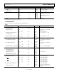
Table 9. ADG5233 Truth Table
EN
INx SxA SxB
1 X
1
Off Off
0 0 Off On
0 1 On Off
1
X is don’t care.
V
DD
1
S1A
2
D1
3
S1B
4
GND
16
IN1
15
EN
14
V
SS
13
S2B
5
S3B
12
D2
6
D3
11
S2A
7
S3A
10
IN2
8
IN3
9
ADG5233
TOP VIEW
(Not to Scale)
09919-003
NOTES
1. EXPOSED PAD TIED TO SUBSTRATE, V
SS
.
1D1
2
S1B
3S2B
4D2
11
V
SS
12 EN
10 S3B
9D3
5
S2A
6
IN2
7
IN3
8
S3A
15
V
DD
16
S1A
14
GND
13
IN1
TOP VIEW
(Not to Scale)
ADG5233
09919-004