
Datasheet
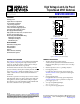


High Voltage Latch-Up Proof,
Triple/Quad SPDT Switches
Data Sheet
ADG5233/ADG5234
Rev. B Document Feedback
Information furnished by Analog Devices is believed to be accurate and reliable. However, no
responsibility is assumed by Analog Devices for its use, nor for any infringements of patents or other
rights of third parties that may result from its use. Specifications subject to change without notice. No
license is granted by implication or otherwise under any patent or patent rights of Analog Devices.
Trademarks and registered trademarks are the property of their respective owners.
One Technology Way, P.O. Box 9106, Norwood, MA 02062-9106, U.S.A.
Tel: 781.329.4700 ©2011–2013 Analog Devices, Inc. All rights reserved.
Technical Support www.analog.com
FEATURES
Latch-up proof
4.5 pF off source capacitance
10 pF off drain capacitance
−0.6 pC charge injection
Low on resistance: 160 Ω typical
±9 V to ±22 V dual-supply operation
9 V to 40 V single-supply operation
48 V supply maximum ratings
Fully specified at ±15 V, ±20 V, +12 V, and +36 V
V
DD
to V
SS
analog signal range
Human body model (HBM) ESD rating
4 kV I/O port to supplies
1 kV I/O port to I/O port
4 kV all other pins
APPLICATIONS
Automatic test equipment
Data acquisition
Instrumentation
Avionics
Audio and video switching
Communication systems
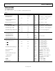
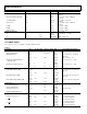
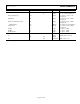
FUNCTIONAL BLOCK DIAGRAMS
Figure 1. ADG5233 TSSOP and LFCSP_WQ
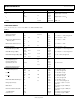
Figure 2. ADG5234 TSSOP and LFCSP_WQ
GENERAL DESCRIPTION
The ADG5233 and ADG5234 are monolithic industrial CMOS
analog switches comprising three independently selectable
single-pole, double throw (SPDT) switches and four indepen-
dently selectable SPDT switches, respectively.
All channels exhibit break-before-make switching action that
prevents momentary shorting when switching channels. An
EN
input on the ADG5233 (LFCSP and TSSOP packages) is used to
enable or disable the device. When disabled, all channels are
switched off.
The ultralow capacitance and charge injection of these switches
make them ideal solutions for data acquisition and sample-and-
hold applications, where low glitch and fast settling are required.
Fast switching speed coupled with high signal bandwidth make
these devices suitable for video signal switching.
PRODUCT HIGHLIGHTS
1. Trench Isolation Guards Against Latch-Up.
A dielectric trench separates the P and N channel transistors
thereby preventing latch-up even under severe overvoltage
conditions.
2. Ultralow Capacitance and −0.6 pC Charge Injection.
3. Dual-Supply Operation.
For applications where the analog signal is bipolar, the
ADG5233/ADG5234 can be operated from dual supplies
up to ±22 V.
4. Single-Supply Operation.
For applications where the analog signal is unipolar, the
ADG5233/ADG5234 can be operated from a single-rail
power supply up to 40 V.
5. 3 V Logic-Compatible Digital Inputs.
V
INH
= 2.0 V, V
INL
= 0.8 V.
6. No V
L
Logic Power Supply Required.
S1A
D1
S1B
S3B
D3
S3A
S2B
D2
S2A
ADG5233
IN1 IN2 IN3 EN
LOGIC
SWITCHES SHOWN FOR
A 1 INPUT LOGIC.
09919-001
ADG5234
SWITCHES SHOWN FOR
A 1 INPUT LOGIC.
S
1
A
D1
IN1
S1B
S2B
D2
IN2
S
2
A
S4A
D4
IN4
S4B
S3B
D3
IN3
S3A
09919-002