
Datasheet

ADG451/ADG452/ADG453
Rev. C | Page 12 of 16
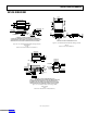
APPLICATIONS
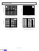
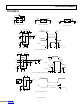
Figure 15 illustrates a precise, fast, sample-and-hold circuit. An
AD845 is used as the input buffer, and the output operational
amplifier is an
AD711. During track mode, SW1 is closed, and
the output, V
OUT
, follows the input signal, V
IN
. In hold mode,
SW1 is opened, and the signal is held by the hold capacitor, C
H
.
SD
V
OUT
SD
–15V
+15V +5V
C
C
1000pF
2200pF
R
C
75Ω
1213
45
SW1
ADG451/
ADG452/
ADG453
–15V
+15V
V
IN
AD845
–15V
+15V
AD711
SW2
CH
2200pF
05239-013
Figure 15. Fast, Accurate Sample-and-Hold Circuit
Due to switch and capacitor leakage, the voltage on the hold
capacitor decreases with time. The ADG451/ADG452/ADG453
minimize this droop due to their low leakage specifications. The
droop rate is further minimized by the use of a polystyrene
hold capacitor. The droop rate for the circuit shown is typically
30 μV/μs.
A second switch, SW2, which operates in parallel with SW1, is
included in this circuit to reduce pedestal error. Because both
switches are at the same potential, they have a differential effect
on the op amp,
AD711, which minimizes charge injection
effects. Pedestal error is also reduced by the compensation
network, R
C
and C
C
. This compensation network reduces the
hold time glitch while optimizing the acquisition time. Using
the illustrated op amps and component values, the pedestal
error has a maximum value of 5 mV over the ±10 V input
range. Both the acquisition and settling times are 850 ns.
Downloaded from Arrow.com.Downloaded from Arrow.com.Downloaded from Arrow.com.Downloaded from Arrow.com.Downloaded from Arrow.com.Downloaded from Arrow.com.Downloaded from Arrow.com.Downloaded from Arrow.com.Downloaded from Arrow.com.Downloaded from Arrow.com.Downloaded from Arrow.com.Downloaded from Arrow.com.