
Datasheet


ADG406/ADG407/ADG426
Rev. B | Page 7 of 20
ADG426 TIMING DIAGRAMS
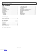
00026-009
50%
50%
2V
0.8V
3
V
0V
3V
A
0, A1, A2, (A3)
EN
0V
t
W
t
S
t
H
WR
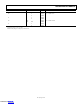
Figure 4. Timing Sequence for Latching the Switch Address and Enable Inputs
Figure 4 shows the timing sequence for latching the switch
address and enable inputs. The latches are level sensitive;
therefore, while
WR
is held low, the latches are transparent and
the switches respond to the address and enable inputs. This
input data is latched on the rising edge of
WR
.
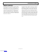
00026-010
3
V
0V
0V
50% 50%
t
W
RS
t
OFF
(RS)
SWITCH
OUTPUT
V
0
0.8V
0
Figure 5. Reset Pulse Width and Reset Turn Off Time
Figure 5 shows the reset pulse width, t
rs
, and the reset turn off
time, t
OFF
(
RS
).
Note that all digital input signals rise and fall times are
measured from 10% to 90% of 3 V; t
R
= t
F
= 20 ns.
Downloaded from Arrow.com.Downloaded from Arrow.com.Downloaded from Arrow.com.Downloaded from Arrow.com.Downloaded from Arrow.com.Downloaded from Arrow.com.Downloaded from Arrow.com.