
Datasheet

I
2
C
®
CMOS 8 × 8 Unbuffered Analog
Switch Array with Dual/Single Supplies
ADG2188
Rev. 0
Information furnished by Analog Devices is believed to be accurate and reliable. However, no
responsibility is assumed by Analog Devices for its use, nor for any infringements of patents or other
rights of third parties that may result from its use. Specifications subject to change without notice. No
license is granted by implication or otherwise under any patent or patent rights of Analog Devices.
Trademarks and registered trademarks are the property of their respective owners.
One Technology Way, P.O. Box 9106, Norwood, MA 02062-9106, U.S.A.
Tel: 781.329.4700 www.analog.com
Fax: 781.461.3113 ©2006 Analog Devices, Inc. All rights reserved.
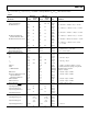
FEATURES
I
2
C-compatible interface
3.4 MHz high speed I
2
C option
32-lead LFCSP_VQ (5 mm × 5 mm)
Double-buffered input logic
Simultaneous update of multiple switches
Up to 300 MHz bandwidth
Fully specified at dual ±5 V/single +12 V operation
On resistance 35 Ω maximum
Low quiescent current < 20 μA
APPLICATIONS
AV switching in TV
Automotive infotainment
AV receivers
CCTV
Ultrasound applications
KVM switching
Telecom applications
Test equipment/instrumentation
PBX systems
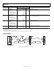
GENERAL DESCRIPTION
The ADG2188 is an analog cross point switch with an
array size of 8 × 8. The switch array is arranged so that
there are eight columns by eight rows, for a total of 64
switch channels. The array is bidirectional, and the rows and
columns can be configured as either inputs or outputs. Each
of the 64 switches can be addressed and configured through
the I
2
C-compatible interface. Standard, full speed, and high
speed (3.4 MHz) I
2
C interfaces are supported. Any
simultaneous switch combination is allowed. An additional
feature of the ADG2188 is that switches can be updated
simultaneously, using the LDSW command. In addition,
a
RESET
option allows all of the switch channels to be
reset/off. At power on, all switches are in the off condition.
The device is packaged in a 32-lead, 5 mm × 5 mm
LFCSP_VQ.
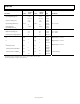
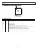
FUNCTIONAL BLOCK DIAGRAM
ADG2188
V
DD
V
SS
V
L
SCL
SD
A
X0 TO X7 (I/O)
8 × 8 SWITCH ARRAY
LDSW
64
1
64
1
INPUT
REGISTER
AND
7 TO 64
DECODER
LATCHES
LDSW
GNDA0A1A2
Y0 TO Y7 (I/O)
0
5897-001
Figure 1.