
Datasheet

Data Sheet ADG1606/ADG1607
Rev. A | Page 9 of 22
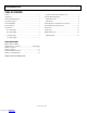
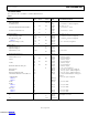
PIN CONFIGURATIONS AND FUNCTION DESCRIPTIONS
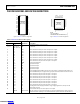
08489-003
NC = NO CONNECT
1
2
3
4
5
6
7
8
9
10
1
1
12
13
14
28
27
26
25
24
23
22
21
20
19
18
17
16
15
NC
NC
S16
S13
S14
S15
V
DD
V
SS
S8
S7
S4
S5
S6
S12
S
1
1
S10
A3
GND
S9
S3
S2
S1
A2
NC
A1
A0
EN
D
ADG1606
T
O
P VIEW
(Not to Scale)
Figure 3. ADG1606 TSSOP Pin Configuration
NOTES
1. NC = NO CONNECT.
2. EXPOSED PAD TIED TO SUBSTRA
TE, V
SS
.
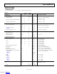
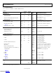
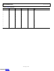
S16
S15
S14
S13
S12
S11
S10
S9
S8
S7
S6
S5
S4
S3
S2
S1
GND
A3
A2
NC
NC
A1
A0
EN
NC
V
DD
NC
D
NC
NC
NC
V
SS
24
23
22
21
20
19
18
17
1
2
3
4
5
6
7
8
9
10
11
12
13
14
15
16
32
31
30
29
28
27
26
25
ADG1606
TOP VIEW
(Not to Scale)
08489-004
Figure 4. ADG1606 LFCSP Pin Configuration
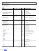
Table 9. ADG1606 Pin Function Descriptions
Pin No.
TSSOP LFCSP Mnemonic Description
1 31 V
DD
Most Positive Power Supply Potential.
2, 3, 13 12, 13, 26,
27, 28, 30, 32
NC No Connect.
4 1 S16 Source Terminal 16. This pin can be an input or an output.
5 2 S15 Source Terminal 15. This pin can be an input or an output.
6 3 S14 Source Terminal 14. This pin can be an input or an output.
7
4
S13
Source Terminal 13. This pin can be an input or an output.
8 5 S12 Source Terminal 12. This pin can be an input or an output.
9 6 S11 Source Terminal 11. This pin can be an input or an output.
10 7 S10 Source Terminal 10. This pin can be an input or an output.
11 8 S9 Source Terminal 9. This pin can be an input or an output.
12 9 GND Ground (0 V) Reference.
14 10 A3 Logic Control Input.
15 11 A2 Logic Control Input.
16 14 A1 Logic Control Input.
17 15 A0 Logic Control Input.
18 16 EN Active High Digital Input. When this pin is low, the device is disabled and all switches are
turned off. When this pin is high, the Ax logic inputs determine which switch is turned on.
19 17 S1 Source Terminal 1. This pin can be an input or an output.
20 18 S2 Source Terminal 2. This pin can be an input or an output.
21 19 S3 Source Terminal 3. This pin can be an input or an output.
22 20 S4 Source Terminal 4. This pin can be an input or an output.
23 21 S5 Source Terminal 5. This pin can be an input or an output.
24 22 S6 Source Terminal 6. This pin can be an input or an output.
25 23 S7 Source Terminal 7. This pin can be an input or an output.
26 24 S8 Source Terminal 8. This pin can be an input or an output.
27 25 V
SS
Most Negative Power Supply Potential. In single-supply applications, this pin can be
connected to ground.
28 29 D Drain Terminal. This pin can be an input or an output.
EPAD Exposed Pad The exposed pad is connected internally. For increased reliability of the solder joints and
maximum thermal capability, it is recommended that the pad be soldered to the substrate, V
SS
.
Downloaded from Arrow.com.Downloaded from Arrow.com.Downloaded from Arrow.com.Downloaded from Arrow.com.Downloaded from Arrow.com.Downloaded from Arrow.com.Downloaded from Arrow.com.Downloaded from Arrow.com.Downloaded from Arrow.com.