
Datasheet
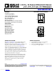

4.5 Ω RON, 16-Channel, Differential 8-Channel,
±5 V,+12 V,+5 V, and +3.3 V Multiplexers
Data Sheet
ADG1606/ADG1607
Rev. A Document Feedback
Information furnished by Analog Devices is believed to be accurate and reliable. However, no
responsibility is assumed by Analog Devices for its use, nor for any infringements of patents or other
rights of third parties that may result from its use. Specifications subject to change without notice. No
license is granted by implication or otherwise under any patent or patent rights of Analog Devices.
Trademarks and registered trademarks are the property of their respective owners.
One Technology Way, P.O. Box 9106, Norwood, MA 02062-9106, U.S.A.
Tel: 781.329.4700 ©2009–2016 Analog Devices, Inc. All rights reserved.
Technical Support www.analog.com
FEATURES
4.5 Ω typical on resistance
1.1 Ω on resistance flatness
±3.3 V to ±8 V dual supply operation
3.3 V to 16 V single supply operation
No V
L
supply required
3 V logic-compatible inputs
Rail-to-rail operation
Up to 378 mA of continuous current per channel
28-lead TSSOP and 32-lead, 5 mm × 5 mm LFCSP
APPLICATIONS
Communication systems
Medical systems
Audio signal routing
Video signal routing
Automatic test equipment
Data acquisition systems
Battery-powered systems
Sample-and-hold systems
Relay replacements
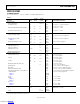
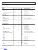
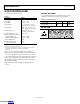
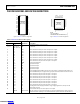
FUNCTIONAL BLOCK DIAGRAMS
1-OF-16
DECODER
A0 A1 A2
A3
EN
ADG1606
S1
S16
D
08489-001
Figure 1.
1-OF-8
DECODER
A0
A1 A2
EN
ADG1607
S1B
S8B
DB
S1A
S8A
DA
08489-002
Figure 2.
GENERAL DESCRIPTION
The ADG1606 and ADG1607 are monolithic iCMOS® analog
multiplexers comprising of 16 single channels and eight
differential channels, respectively. The ADG1606 switches one of
16 inputs to a common output, as determined by the 4-bit
binary address lines (A0, A1, A2, and A3). The ADG1607
switches one of eight differential inputs to a common differential
output, as determined by the 3-bit binary address lines (A0, A1,
and A2). An EN input on both devices enables or disables the
device. When disabled, all channels switch off. When enabled,
each channel conducts equally well in both directions and has an
input signal range that extends to the supplies.
The ultralow on resistance and on-resistance flatness of these
switches make them ideal solutions for data acquisition and
gain switching applications where low distortion is critical.
iCMOS® construction ensures ultralow power dissipation,
making the parts ideally suited for portable and battery-
powered instruments.
PRODUCT HIGHLIGHTS
1. 7.5 Ω maximum on resistance over temperature.
2. Minimum distortion: THD + N = 0.04%
3. 3 V logic-compatible digital inputs: V
INH
= 2.0 V, V
INL
= 0.8 V.
4. No V
L
logic power supply required.
Downloaded from Arrow.com.