
Datasheet
ADG1411/ADG1412/ADG1413 Data Sheet
Rev. C | Page 6 of 16
ABSOLUTE MAXIMUM RATINGS
T
A
= 25°C, unless otherwise noted.
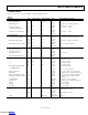
Table 4.
Parameter Rating
V
DD
to V
SS
35 V
V
DD
to GND −0.3 V to +25 V
V
SS
to GND +0.3 V to −25 V
Analog Inputs
1
V
SS
− 0.3 V to V
DD
+ 0.3 V or
30 mA, whichever occurs first
Digital Inputs
1
GND − 0.3 V to V
DD
+ 0.3 V or
30 mA, whichever occurs first
Peak Current, Sx or Dx Pins 500 mA (pulsed at 1 ms,
10% duty cycle maximum)
Continuous Current per
Channel at 25°C
16-Lead TSSOP 190 mA
16-Lead LFCSP 250 mA
Continuous Current per
Channel at 125°C
16-Lead TSSOP 90 mA
16-Lead LFCSP 100 mA
Operating Temperature Range
Automotive (Y Version) −40°C to +125°C
Storage Temperature Range −65°C to +150°C
Junction Temperature 150°C
θ
JA
Thermal Impedance
16-Lead TSSOP (4-Layer Board) 112°C/W
16-Lead LFCSP 30.4°C/W
Reflow Soldering Peak
Temperature, Pb Free
260(+0/−5)°C
1
Overvoltages at the INx, Sx, and Dx pins are clamped by internal diodes.
Current should be limited to the maximum ratings given.
Stresses at or above those listed under Absolute Maximum
Ratings may cause permanent damage to the product. This is a
stress rating only; functional operation of the product at these
or any other conditions above those indicated in the operational
section of this specification is not implied. Operation beyond
the maximum operating conditions for extended periods may
affect product reliability.
Only one absolute maximum rating may be applied at any
one time.
ESD CAUTION
Downloaded from Arrow.com.Downloaded from Arrow.com.Downloaded from Arrow.com.Downloaded from Arrow.com.Downloaded from Arrow.com.Downloaded from Arrow.com.