
Datasheet


ADF4153A Data Sheet
Rev. A | Page 20 of 24
ADuC812 Interface
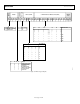
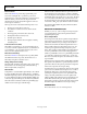
Figure 23 shows the interface between the ADF4153A and the
ADuC812 MicroConverter®. Because the ADuC812 is based on
an 8051 core, this interface can be used with any 8051-based
microcontroller. The MicroConverter is set up for SPI master
mode with CPHA = 0. To initiate the operation, the I/O port
driving LE is brought low. Each latch of the ADF4153A needs a
24-bit word, which is accomplished by writing three 8-bit bytes
from the MicroConverter to the device. After the third byte is
written, the LE input should be brought high to complete the
transfer.
ADuC812
ADF4153A
SCLOCK
CLK
DATA
LE
MUXOUT
(LOCK DETECT)
MOSI
I/O PORTS
11047-023
Figure 23. ADuC812 to ADF4153A Interface
When operating in this mode, the maximum SCLOCK rate of
the ADuC812 is 4 MHz. This means that the maximum rate at
which the output frequency can be changed is 180 kHz.
ADSP-21xx Interface
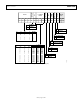
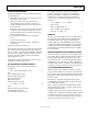
Figure 24 shows the interface between the ADF4153A and the
ADSP-21xx digital signal processor. As discussed previously,
the ADF4153A needs a 24-bit serial word for each latch write.
The easiest way to accomplish this using the ADSP-21xx family
is to use the autobuffered transmit mode of operation with
alternate framing. This provides a means for transmitting an
entire block of serial data before an interrupt is generated.
Set up the word length for eight bits and use three memory
locations for each 24-bit word. To program each 24-bit latch,
store the three 8-bit bytes, enable the autobuffered mode, and
write to the transmit register of the DSP. This last operation
initiates the autobuffer transfer.
ADSP-21xx
ADF4153A
SCLK CLK
DATA
LE
MUXOUT
(LOCK DETECT)
DT
TFS
I/O FLAGS
11047-024
Figure 24. ADSP-21xx to ADF4153A Interface
PCB DESIGN GUIDELINES FOR CHIP SCALE
PACKAGE
The lands on the chip scale package (CP-20) are rectangular.
The printed circuit board (PCB) pad for these should be 0.1 mm
longer than the package land length and 0.05 mm wider than
the package land width. The land should be centered on the
pad. This ensures that the solder joint size is maximized.
The bottom of the chip scale package has a central thermal pad.
The thermal pad on the PCB should be at least as large as this
exposed pad. On the PCB, there should be a clearance of at least
0.25 mm between the thermal pad and the inner edges of the
pad pattern. This ensures that shorting is avoided.
Thermal vias can be used on the PCB thermal pad to improve
thermal performance of the package. If vias are used, they should
be incorporated in the thermal pad at 1.2 mm pitch grid. The
via diameter should be between 0.3 mm and 0.33 mm, and the
via barrel should be plated with one ounce of copper to plug the
via. The user should connect the PDB thermal pad to AGND.