
Datasheet


Data Sheet ADF4153A
Rev. A | Page 19 of 24
Reference Spurs
Reference spurs are generally not a problem in fractional-N
synthesizers because the reference offset is far outside the
loop bandwidth. However, any reference feedthrough mechan-
ism that bypasses the loop can cause a problem. One such
mechanism is feedthrough of low levels of on-chip reference
switching noise out through the RF
IN
pin back to the VCO,
resulting in reference spur levels as high as –90 dBc. Ensure that
in the PCB layout that the VCO is well separated from the input
reference to avoid a possible feed-through path on the board.
SPUR CONSISTENCY
When jumping from Frequency A to Frequency B and then
back again using some fractional-N synthesizers, the spur levels
often differ each time Frequency A is programmed. However,
in the ADF4153A, the spur levels on any particular channel are
always consistent.
PHASE RESYNC
The output of a fractional-N PLL can settle to any one of MOD
phase offsets with respect to the input reference, where MOD
is the fractional modulus. The phase resync feature in the
ADF4153A can be used to produce a consistent output phase
offset with respect to the input reference. This is necessary
in applications where the output phase and frequency are
important, such as digital beam-forming.
When phase resync is enabled, an internal timer generates sync
signals at intervals of t
SYNC
given by the following formula:
t
SYNC
= RESYNC × RESYNC_DELAY × t
PFD
where t
PFD
is the PFD reference period.
RESYNC is the decimal value programmed in Bits DB[15…12]
of Register R2 and can be any integer in the range of 1 to 15. If
RESYNC is programmed to its default value of all zeros, then
the phase resync feature is disabled.
If phase resync is enabled, then RESYNC_DELAY must be
programmed to a value that is an integer multiple of the value
of MOD. RESYNC_DELAY is the decimal value programmed
into the MOD bits (DB[13…2] of Register R1 when load
control (Bit DB23 of Register R1) = 1.
When a new frequency is programmed, the second next sync
pulse after the LE rising edge is used to resynchronize the output
phase to the reference. The t
SYNC
time should be programmed to
a value that is at least as long as the worst-case lock time. Doing
so guarantees that the phase resync occurs after the last cycle
slip in the PLL settling transient.
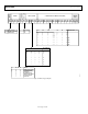
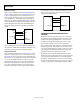
In the example shown in Figure 22, the PFD reference is
25 MHz and MOD = 125 for a 200 kHz channel spacing.
t
SYNC
is set to 400 µs by programming RESYNC = 10 and
RESYNC_DELAY = 1000.
LE
PHASE
FREQUENCY
SYNC
(INTERNAL)
–100 0
100 200 1000
300 400 500 600 700 800
900
TIME (µs)
PLL SETTLES TO
CORRECT PHASE
AFTER RESYNC
LAST CYCLE SLIP
PLL SETTLES TO
INCORRECT PHASE
t
SYNC
11047-022
Figure 22. Phase Resync Example
FILTER DESIGN—ADIsimPLL
A filter design and analysis program is available to help the user
implement PLL design. Visit www.analog.com/pll for a free
download of the ADIsimPLL™ software. The software designs,
simulates, and analyzes the entire PLL frequency domain and
time domain response. Various passive and active filter
architectures are allowed.
INTERFACING
The ADF4153A has a simple SPI®-compatible serial interface
for writing to the device. CLK, DATA, and LE control the data
transfer. When latch enable (LE) is high, the 22 bits that are
clocked into the input register on each rising edge of SCLK are
transferred to the appropriate latch. See Figure 2 for the timing
diagram and Table 5 for the register truth table.
The maximum allowable serial clock rate is 20 MHz.