
Datasheet


ADF4153A Data Sheet
Rev. A | Page 16 of 24
RF Power-Down
DB4 on the ADF4153A provides the programmable power-
down mode. Setting this bit to 1 performs a power-down.
Setting this bit to 0 returns the synthesizer to normal operation.
While in software power-down mode, the part retains all
information in its registers. Only when supplies are removed
are the register contents lost.
When a power-down is activated, the following events occur:
1. All active dc current paths are removed.
2. The synthesizer counters are forced to their load state
conditions.
3. The charge pump is forced into three-state mode.
4. The digital lock detect circuitry is reset.
5. The RF
IN
input is debiased.
6. The input register remains active and capable of loading
and latching data.
Lock Detect Precision (LDP)
When DB5 is programmed to 0, 24 consecutive PFD cycles of
15 ns must occur before digital lock detect is set. When this bit
is programmed to 1, 40 consecutive reference cycles of 15 ns
must occur before digital lock detect is set.
Phase Detector Polarity
DB6 in the ADF4153A sets the phase detector polarity. When
the VCO characteristics are positive, this should be set to 1.
When they are negative, it should be set to 0.
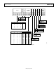
Charge Pump Current Setting
DB7, DB8, DB9, and DB10 set the charge pump current setting.
This should be set to the charge pump current that the loop
filter is designed with (see Figure 19).
REF
IN
Doubler
Setting DB11 to 0 feeds the REF
IN
signal directly to the 4-bit RF
R counter, disabling the doubler. Setting this bit to 1 multiplies
the REF
IN
frequency by a factor of 2 before feeding into the 4-bit
R counter. When the doubler is disabled, the REF
IN
falling edge
is the active edge at the PFD input to the fractional synthesizer.
When the doubler is enabled, both the rising and falling edges
of REF
IN
become active edges at the PFD input.
When the doubler is enabled and the lowest spur mode is chosen,
the in-band phase noise performance is sensitive to the REF
IN
duty cycle. The phase noise degradation can be as much as 5 dB
for the REF
IN
duty cycles outside a 45% to 55% range. The phase
noise is insensitive to the REF
IN
duty cycle in the lowest noise
mode and in the lowest noise and spur mode. The phase noise
is insensitive to REF
IN
duty cycle when the doubler is disabled.
The maximum allowed REF
IN
frequency when the doubler is
enabled is 30 MHz.
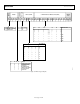
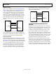
NOISE AND SPUR REGISTER, R3
With R3[1, 0] set to [1, 1], the on-chip noise and spur register
is programmed. Figure 20 shows the input data format for
programming this register.
Noise and Spur Mode
Noise and spur mode lets the user optimize a design either for
improved spurious performance or for improved phase noise
performance. When the low spur setting is chosen, dither is
enabled. This randomizes the fractional quantization noise so
that it resembles white noise rather than spurious noise. As a
result, the part is optimized for improved spurious perfor-
mance. This operation would normally be used when the PLL
closed-loop bandwidth is wide, for fast-locking applications.
(Wide-loop bandwidth is seen as a loop bandwidth greater than
1/10 of the RF
OUT
channel step resolution (f
RES
).) A wide-loop
filter does not attenuate the spurs to the same level as a narrow-
loop bandwidth.
When the low noise and spur setting is enabled, dither is disabled.
This optimizes the synthesizer to operate with improved noise
performance. However, the spurious performance is degraded
in this mode compared to the low spur setting.
To further improve noise performance, the lowest noise setting
option can be used, which reduces the phase noise. As well as
disabling the dither, it also ensures that the charge pump is
operating in an optimum region for noise performance. This
setting is extremely useful where a narrow-loop filter band-
width is available. The synthesizer ensures extremely low noise
and the filter attenuates the spurs. The typical performance
characteristics give the user an idea of the trade-off in a typical
W-CDMA setup for the different noise and spur settings.
RESERVED BITS
These bits should be set to 0 for normal operation.