
Datasheet


ADCLK954
Rev. B | Page 6 of 12
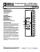
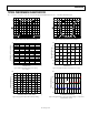
PIN CONFIGURATION AND FUNCTION DESCRIPTIONS
NOTES
1. EPAD MUST BE SOLDERED TO V
EE
POWER PLANE.
1IN_SEL
2CLK0
3CLK0
4V
REF
0
5V
T
0
6CLK1
7CLK1
8V
T
1
9V
REF
1
10V
EE
23 Q7
24 Q6
25 Q6
26 Q5
27 Q5
28 Q4
29 Q4
30 V
CC
22 Q7
21 V
CC
11
V
CC
12
Q11
13
Q11
15
Q10
17
Q9
16
Q9
18
Q8
19
Q8
20
V
CC
14
Q
10
33
Q3
34
Q2
35
Q2
36
Q1
37
Q1
38
Q0
39
Q0
40
V
CC
32
Q3
31
V
CC
TOP VIEW
(Not to Scale)
ADCLK954
07968-002
Figure 2. Pin Configuration
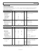
Table 7. Pin Function Descriptions
Pin No. Mnemonic Description
1 IN_SEL
Input Select. Logic 0 selects CLK0 and CLK0
inputs. Logic 1 selects CLK1 and CLK1 inputs.
2 CLK0 Differential Input (Positive) 0.
3
CLK0
Differential Input (Negative) 0.
4 V
REF
0
Reference Voltage. Reference voltage for biasing ac-coupled CLK0 and CLK0
inputs.
5 V
T
0
Center Tap. Center tap of a 100 Ω input resistor for CLK0 and CLK0
inputs.
6 CLK1 Differential Input (Positive) 1.
7
CLK1
Differential Input (Negative) 1.
8 V
T
1
Center Tap. Center tap of a 100 Ω input resistor for CLK1 and CLK1
inputs.
9 V
REF
1
Reference Voltage. Reference voltage for biasing ac-coupled CLK1 and CLK1
inputs.
10 V
EE
Negative Supply Pin.
11, 20, 21,
30, 31, 40
V
CC
Positive Supply Pin.
12, 13
Q11
, Q11
Differential LVPECL Outputs.
14, 15
Q10
, Q10
Differential LVPECL Outputs.
16, 17
Q9
, Q9
Differential LVPECL Outputs.
18, 19
Q8
, Q8
Differential LVPECL Outputs.
22, 23
Q7
, Q7
Differential LVPECL Outputs.
24, 25
Q6
, Q6
Differential LVPECL Outputs.
26, 27
Q5
, Q5
Differential LVPECL Outputs.
28, 29
Q4
, Q4
Differential LVPECL Outputs.
32, 33
Q3
, Q3
Differential LVPECL Outputs.
34, 35
Q2
, Q2
Differential LVPECL Outputs.
36, 37
Q1
, Q1
Differential LVPECL Outputs.
38, 39
Q0
, Q0
Differential LVPECL Outputs.
EPAD Exposed pad (EPAD) must be connected to V
EE
.