
Datasheet
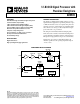


Table Of Contents
- FEATURES
- APPLICATIONS
- GENERAL DESCRIPTION
- FUNCTIONAL BLOCK DIAGRAM
- TABLE OF CONTENTS
- REVISION HISTORY
- SPECIFICATIONS
- ABSOLUTE MAXIMUM RATINGS
- PIN CONFIGURATION AND FUNCTION DESCRIPTIONS
- TERMINOLOGY
- EQUIVALENT INPUT/OUTPUT CIRCUITS
- TYPICAL PERFORMANCE CHARACTERISTICS
- SYSTEM OVERVIEW
- SERIAL INTERFACE TIMING
- COMPLETE REGISTER LISTING
- PRECISION TIMING HIGH SPEED TIMING GENERATION
- HORIZONTAL CLAMPING AND BLANKING
- GENERATING SPECIAL HBLK PATTERNS
- POWER-UP PROCEDURE
- ANALOG FRONT END DESCRIPTION AND OPERATION
- APPLICATIONS INFORMATION
- OUTLINE DIMENSIONS
AD9949
Rev. B | Page 3 of 36
SPECIFICATIONS
GENERAL SPECIFICATIONS
Table 1.
Parameter Min Typ Max Unit
TEMPERATURE RANGE
Operating −20 +85 °C
Storage −65 +150 °C
MAXIMUM CLOCK RATE 36 MHz
POWER SUPPLY VOLTAGE
AVDD, TCVDD (AFE, Timing Core) 2.7 3.0 3.6 V
HVDD (H1 to H4 Drivers) 2.7 3.0 3.6 V
RGVDD (RG Driver) 2.7 3.0 3.6 V
DRVDD (D0 to D11 Drivers) 2.7 3.0 3.6 V
DVDD (All Other Digital) 2.7 3.0 3.6 V
POWER DISSIPATION
36 MHz, HVDD = RGVDD = 3 V, 100 pF H1 to H4 Loading
1
320 mW
Total Shutdown Mode 1 mW
1
The total power dissipated by the HVDD supply may be approximated using the equation
Total HVDD Power = (CLOAD x HVDD x Pixel Frequency) x HVDD x (Number of H – Outputs Used)
Reducing the H-loading, using only two of the outputs, and/or using a lower HVDD supply, reduces the power dissipation.
DIGITAL SPECIFICATIONS
T
MIN
to T
MAX
, AVDD = DVDD = DRVDD = HVDD = RGVDD = 2.7 V, C
L
= 20 pF, unless otherwise noted.
Table 2.
Parameter Symbol Min Typ Max Unit
LOGIC INPUTS
High Level Input Voltage V
IH
2.1 V
Low Level Input Voltage V
IL
0.6 V
High Level Input Current I
IH
10 µA
Low Level Input Current I
IL
10 µA
Input Capacitance C
IN
10 pF
LOGIC OUTPUTS
High Level Output Voltage, I
OH
= 2 mA V
OH
2.2 V
Low Level Output Voltage, I
OL
= 2 mA V
OL
0.5 V
CLI INPUT
High Level Input Voltage
(TCVDD/2 + 0.5 V) V
IH–CLI
1.85 V
Low Level Input Voltage V
IL–CLI
0.85 V
RG AND H-DRIVER OUTPUTS
High Level Output Voltage
(RGVDD – 0.5 V and HVDD – 0.5 V) V
OH
2.2 V
Low Level Output Voltage V
OL
0.5 V
Maximum Output Current (Programmable) 30 mA
Maximum Load Capacitance 100 pF