
Datasheet


Table Of Contents
- FEATURES
- APPLICATIONS
- GENERAL DESCRIPTION
- FUNCTIONAL BLOCK DIAGRAM
- TABLE OF CONTENTS
- REVISION HISTORY
- SPECIFICATIONS
- ABSOLUTE MAXIMUM RATINGS
- PIN CONFIGURATION AND FUNCTION DESCRIPTIONS
- TERMINOLOGY
- EQUIVALENT INPUT/OUTPUT CIRCUITS
- TYPICAL PERFORMANCE CHARACTERISTICS
- SYSTEM OVERVIEW
- SERIAL INTERFACE TIMING
- COMPLETE REGISTER LISTING
- PRECISION TIMING HIGH SPEED TIMING GENERATION
- HORIZONTAL CLAMPING AND BLANKING
- GENERATING SPECIAL HBLK PATTERNS
- POWER-UP PROCEDURE
- ANALOG FRONT END DESCRIPTION AND OPERATION
- APPLICATIONS INFORMATION
- OUTLINE DIMENSIONS
AD9949
Rev. B | Page 25 of 36
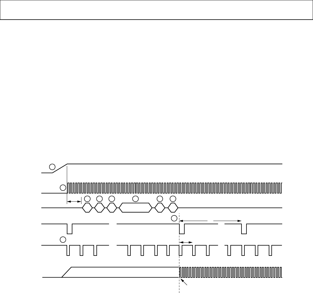
POWER-UP PROCEDURE
RECOMMENDED POWER-UP SEQUENCE
When the AD9949 is powered up, the following sequence is
recommended (refer to Figure 27 for each step):
1. Turn on the power supplies for the AD9949.
2. Apply the master clock input, CLI, VD, and HD.
3. Although the AD9949 contains an on-chip, power-on reset,
a software reset of the internal registers is recommended.
Write a 1 to the SW_RST register (Address 0×10), which
resets the internal registers to their default values. This bit
is self-clearing and automatically resets back to 0.
4. The Precision Timing core must be reset by writing a 0 to
the TGCORE_RSTB register (Address 0×12) followed by
writing a l to the TGCORE_RSTB register. This starts the
internal timing core operation.
5. Write a 1 to the PREVENTUPDATE register (Address
0×14). This prevents the updating of the serial register
data.
6. Write to the desired registers to configure high speed
timing and horizontal timing.
7. Write a 1 to the OUT_CONTROL register (Address 0×11).
This allows the outputs to become active after the next
VD/HD rising edge.
8. Write a 0 to the PREVENTUPDATE register (Address
0×14). This allows the serial information to be updated at
next VD/HD falling edge.
9. The next VD/HD falling edge allows register updates to
occur, including OUT_CONTROL, which enables all clock
outputs.
VDD
(INPUT)
SERIAL
WRITES
VD
(OUTPUT)
1H
ODD FIELD EVEN FIELD
...
...
DIGITAL
OUTPUTS
CLOCKS ACTIVE WHEN OUT_CONTROL REGISTER IS
UPDATED AT VD/HD EDGE
H1/H3, RG
H2/H4
t
PWR
CLI
(INPUT)
HD
(OUTPUT)
1V
...
...
03751-028
1
2
2
3 4 5 6 7 8
9
Figure 27. Recommended Power-Up Sequence