
Datasheet
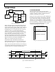
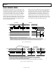

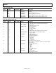
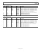
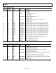

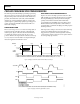

Table Of Contents
- FEATURES
- APPLICATIONS
- GENERAL DESCRIPTION
- FUNCTIONAL BLOCK DIAGRAM
- TABLE OF CONTENTS
- REVISION HISTORY
- SPECIFICATIONS
- ABSOLUTE MAXIMUM RATINGS
- PIN CONFIGURATION AND FUNCTION DESCRIPTIONS
- TERMINOLOGY
- EQUIVALENT INPUT/OUTPUT CIRCUITS
- TYPICAL PERFORMANCE CHARACTERISTICS
- SYSTEM OVERVIEW
- SERIAL INTERFACE TIMING
- COMPLETE REGISTER LISTING
- PRECISION TIMING HIGH SPEED TIMING GENERATION
- HORIZONTAL CLAMPING AND BLANKING
- GENERATING SPECIAL HBLK PATTERNS
- POWER-UP PROCEDURE
- ANALOG FRONT END DESCRIPTION AND OPERATION
- APPLICATIONS INFORMATION
- OUTLINE DIMENSIONS
AD9949
Rev. B | Page 19 of 36
Table 16. H1CONTROL, RGCONTROL, DRVCONTROL, and SAMPCONTROL Register Parameters
Parameter Length Range Description
Polarity 1b High/Low Polarity Control for H1/H3 and RG (0 = No Inversion, 1 = Inversion).
Positive Edge 6b 0 to 47 Edge Location Positive Edge Location for H1/H3 and RG.
Negative Edge 6b 0 to 47 Edge Location Negative Edge Location for H1/H3 and RG.
Sample Location 6b 0 to 47 Sample Location Sampling Location for SHP and SHD.
Drive Control 3b 0 to 7 Current Steps Drive Current for H1 to H4 and RG Outputs, 0 to 7 Steps of 4.1 mA Each.
DOUT Phase 6b 0 to 47 Edge Location Phase Location of Data Outputs with Respect to Pixel Period.
Table 17. Precision Timing Edge Locations
Quadrant Edge Location (Decimal) Register Value (Decimal) Register Value (Binary)
I 0 to 11 0 to 11 000000 to 001011
II 12 to 23 16 to 27 010000 to 011011
III 24 to 35 32 to 43 100000 to 101011
IV 36 to 47 48 to 59 110000 to 111011
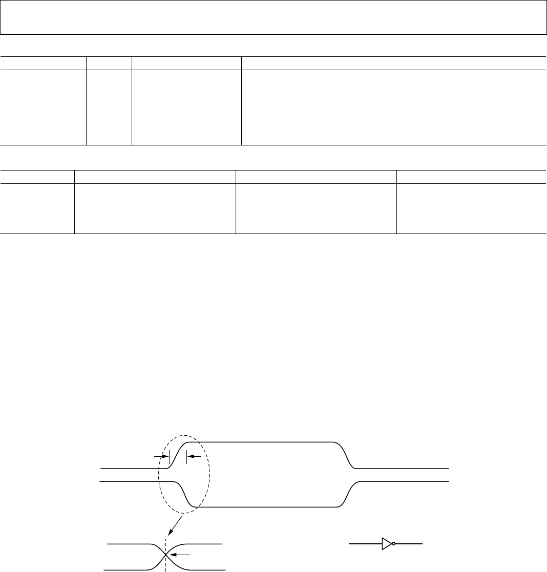
H-DRIVER AND RG OUTPUTS
In addition to the programmable timing positions, the AD9949 features on-chip output drivers for the RG and H1 to H4 outputs. These
drivers are powerful enough to directly drive the CCD inputs. The H-driver and RG driver current can be adjusted for optimum rise/fall
time into a particular load by using the DRVCONTROL register (Address 0×62). The DRVCONTROL register is divided into five differ-
ent 3-bit values, each one being adjustable in 4.1 mA increments. The minimum setting of 0 is equal to OFF or three-state, and the maxi-
mum setting of 7 is equal to 30.1 mA.
As shown in Figure 18, the H2/H4 outputs are inverses of H1/H3. The internal propagation delay resulting from the signal inversion is
less than l ns, which is significantly less than the typical rise time driving the CCD load. This results in a H1/H2 crossover voltage at ap-
proximately 50% of the output swing. The crossover voltage is not programmable.
DIGITAL DATA OUTPUTS
The AD9949 data output phase is programmable using the DOUTPHASE register (Address 0×64). Any edge from 0 to 47 may be pro-
grammed, as shown in Figure 19. The pipeline delay for the digital data output is shown in Figure 20.
FIXED CROSSOVER VOLTAGE
H1/H3 H2/H4
t
PD
H2/H4
H1/H3
t
RISE
t
PD
<<
t
RISE
03751-019
Figure 18. H-Clock Inverse Phase Relationship