
Datasheet
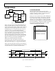
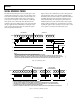

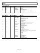
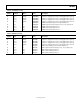
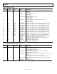


Table Of Contents
- FEATURES
- APPLICATIONS
- GENERAL DESCRIPTION
- FUNCTIONAL BLOCK DIAGRAM
- TABLE OF CONTENTS
- REVISION HISTORY
- SPECIFICATIONS
- ABSOLUTE MAXIMUM RATINGS
- PIN CONFIGURATION AND FUNCTION DESCRIPTIONS
- TERMINOLOGY
- EQUIVALENT INPUT/OUTPUT CIRCUITS
- TYPICAL PERFORMANCE CHARACTERISTICS
- SYSTEM OVERVIEW
- SERIAL INTERFACE TIMING
- COMPLETE REGISTER LISTING
- PRECISION TIMING HIGH SPEED TIMING GENERATION
- HORIZONTAL CLAMPING AND BLANKING
- GENERATING SPECIAL HBLK PATTERNS
- POWER-UP PROCEDURE
- ANALOG FRONT END DESCRIPTION AND OPERATION
- APPLICATIONS INFORMATION
- OUTLINE DIMENSIONS

AD9949
Rev. B | Page 17 of 36
Table 14. AFE Operation Register Detail
Address
Data Bit
Content
Default
Value
Name Description
00 [1:0] 0 PWRDOWN
0 = Normal Operation.
1 = Reference Standby.
2/3 = Total Power-Down
[2] 1 CLPENABLE
0 = Disable OB Clamp.
1 = Enable OB Clamp.
[3] 0 CLPSPEED
0 = Select Normal OB Clamp Settling.
1 = Select Fast OB Clamp Settling.
[4] 0 FASTUPDATE
0 = Ignore VGA Update.
1 = Very Fast Clamping when VGA Is Updated.
[5] 0 PBLK_LVL
DOUT Value during PBLK.
0 = Blank to Zero.
1 = Blank to Clamp Level.
[7:6] 0 TEST MODE Test Operation Only. Set to zero.
[8] 0 DCBYP
0 = Enable DC restore circuit.
1 = Bypass DC Restore Circuit during PBLK.
[9] 0 TESTMODE Test Operation Only. Set to zero.
[11:10] 0 CDSGAIN
Adjustment of CDS Gain.
0 = 0 dB.
01 = −2 dB.
10 = −4 dB.
11 = 0 dB.
Table 15. AFE Control Register Detail
Address
Data Bit
Content
Default
Value
Name Description
03 [1:0] 0 COLORSTEER
0 = Off.
1 = Progressive.
2 = Interlaced.
3 = Three Field.
[2] 1 PxGAENABLE
0 = Disable PxGA.
1 = Enable PxGA.
[3] 0 DOUTDISABLE
0 = Data Outputs Are Driven.
1 = Data Outputs Are Three-Stated.
[4] 0 DOUTLATCH
0 = Latch Data Outputs with DOUT Phase.
1 = Output Latch Transparent.
[5] 0 GRAYENCODE
0 = Binary Encode Data Outputs.
1 = Gray Encode Data Outputs.