
Datasheet
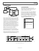
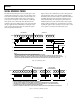

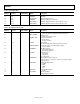
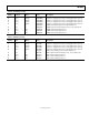

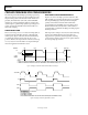

Table Of Contents
- FEATURES
- APPLICATIONS
- GENERAL DESCRIPTION
- FUNCTIONAL BLOCK DIAGRAM
- TABLE OF CONTENTS
- REVISION HISTORY
- SPECIFICATIONS
- ABSOLUTE MAXIMUM RATINGS
- PIN CONFIGURATION AND FUNCTION DESCRIPTIONS
- TERMINOLOGY
- EQUIVALENT INPUT/OUTPUT CIRCUITS
- TYPICAL PERFORMANCE CHARACTERISTICS
- SYSTEM OVERVIEW
- SERIAL INTERFACE TIMING
- COMPLETE REGISTER LISTING
- PRECISION TIMING HIGH SPEED TIMING GENERATION
- HORIZONTAL CLAMPING AND BLANKING
- GENERATING SPECIAL HBLK PATTERNS
- POWER-UP PROCEDURE
- ANALOG FRONT END DESCRIPTION AND OPERATION
- APPLICATIONS INFORMATION
- OUTLINE DIMENSIONS
AD9949
Rev. B | Page 14 of 36
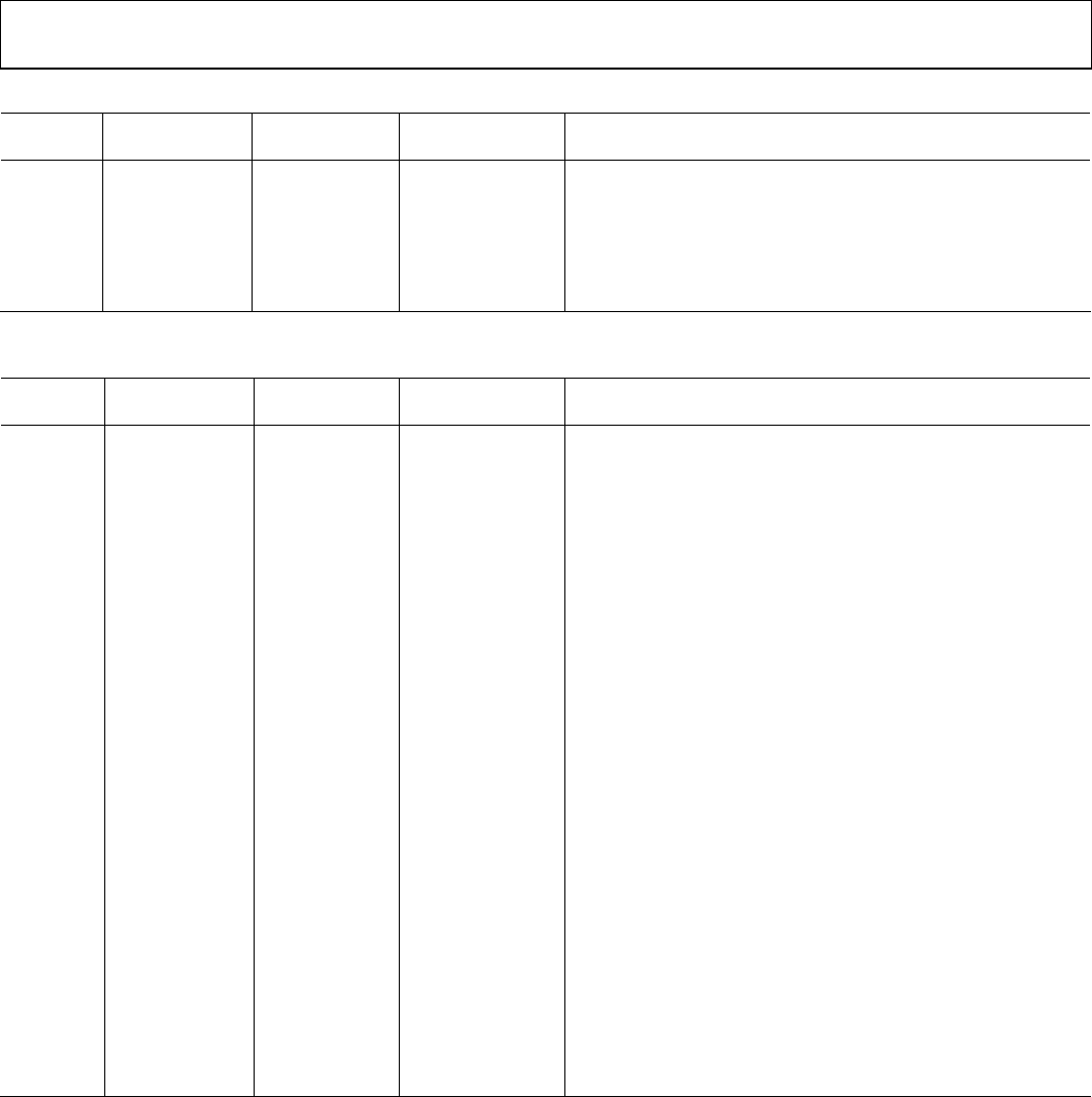
Table 8. AFE Register Map
Address
Data Bit
Content
Default Value Name Description
00 [11:0] 4 OPRMODE AFE Operation Modes. (See Table 14.)
01 [9:0] 0 VGAGAIN VGA Gain.
02 [7:0] 80 CLAMP LEVEL Optical Black Clamp Level.
03 [11:0] 4 CTLMODE AFE Control Modes. (See Table 15.)
04 [17:0] 0 PxGA GAIN01 PxGA Gain Registers for Color 0 [8:0] and Color 1 [17:9].
05 [17:0] 0 PxGA GAIN23 PxGA Gain Registers for Color 2 [8:0] and Color 3 [17:9].
Table 9. Miscellaneous Register Map
Address
Data Bit
Content
Default Value Name Description
10 [0] 0 SW_RST
Software Reset.
1 = Reset all registers to default, then self-clear back to 0.
11 [0] 0 OUT_CONTROL
Output Control.
0 = Make all dc outputs inactive.
12 [0] 0 TGCORE_RSTB
Timing Core Reset Bar.
0 = Reset TG core.
1 = Resume operation.
13 [11:0] 0 UPDATE
Serial Update.
Sets the line (HD) within the field to update serial data.
14 [0] 0 PREVENTUPDATE
Prevents the update of the VD updated registers.
1 = Prevent Update.
15 [0] 0 VDHDEDGE
VD/HD Active Edge.
0 = Falling Edge Triggered.
1 = Rising Edge Triggered.
16 [1:0] 0 FIELDVAL
Field Value Sync.
0 = Next Field 0.
1 = Next Field 1.
2/3 = Next Field 2.
17 [0] 0 HBLKRETIME
Retime HBLK to Internal H1 Clock.
Preferred setting is 1. Setting to 1 adds one cycle delay to HBLK
toggle positions.
18 [1:0] 0 CLPBLKOUT
CLP/BLK Pin Output Select.
0 = CLPOB.
1 = PBLK.
2 = HBLK.
3 = Low.
19 [0] 1 CLPBLKEN
Enable CLP/BLK Output.
1 = Enable.
1A [0] 0 TEST MODE
Internal Test Mode.
Should always be set high.