
Datasheet
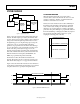
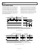

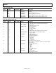
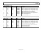

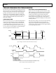

Table Of Contents
- FEATURES
- APPLICATIONS
- GENERAL DESCRIPTION
- FUNCTIONAL BLOCK DIAGRAM
- TABLE OF CONTENTS
- REVISION HISTORY
- SPECIFICATIONS
- ABSOLUTE MAXIMUM RATINGS
- PIN CONFIGURATION AND FUNCTION DESCRIPTIONS
- TERMINOLOGY
- EQUIVALENT INPUT/OUTPUT CIRCUITS
- TYPICAL PERFORMANCE CHARACTERISTICS
- SYSTEM OVERVIEW
- SERIAL INTERFACE TIMING
- COMPLETE REGISTER LISTING
- PRECISION TIMING HIGH SPEED TIMING GENERATION
- HORIZONTAL CLAMPING AND BLANKING
- GENERATING SPECIAL HBLK PATTERNS
- POWER-UP PROCEDURE
- ANALOG FRONT END DESCRIPTION AND OPERATION
- APPLICATIONS INFORMATION
- OUTLINE DIMENSIONS

AD9949
Rev. B | Page 13 of 36
COMPLETE REGISTER LISTING
1. All addresses and default values are expressed in
hexadecimal.
2. All registers are VD/HD updated as shown in Figure 14,
except for the registers indicated in Table 7, which are SL
updated.
Table 7. SL Updated Registers
Register Description
OPRMODE AFE Operation Modes
CTLMODE AFE Control Modes
SW_RESET Software Reset Bit
TGCORE _RSTB Reset Bar Signal for Internal TG Core
PREVENTUPDATE Prevents Update of Registers
VDHDEDGE VD/HD Active Edge
FIELDVAL Resets Internal Field Pulse
HBLKRETIME Retimes the HBLK to Internal Clock
CLPBLKOUT CLP/BLK Output Pin Select
CLPBLKEN Enables CLP/BLK Output Pin
H1CONTROL H1/H2 Polarity/Edge Control
RGCONTROL RG Polarity/Edge Control
DRVCONTROL RG and H1 to H4 Drive Current
SAMPCONTROL SHP/SHD Sampling Edge Control
DOUTPHASE Data Output Phase Adjustment