
Datasheet
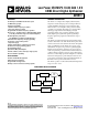


AD9913
Rev. A | Page 7 of 32
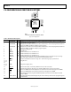
Pin No. Mnemonic I/O Description
26 PWR_DWN_CTL I
External Power-Down, Digital Input (Active High). A high level on this pin initiates the currently
programmed power-down mode. See the Power-Down Features section for further details. If unused,
tie to ground.
27 IO_UPDATE I
I/O Update; Digital Input. A high on this pin indicates a transfer of the contents of the I/O buffers to the
corresponding internal registers.
28
CS
I
Chip Select for Serial and Parallel Port. Digital input (active low). Bringing this pin low enables the
AD9913 to detect serial (SCLK) or parallel (PCLK) clock rising/falling edges. Bringing this pin high
causes the AD9913 to ignore input on the data pins.
29
SDIO(WR
/RD)
I/O Bidirectional Data Line for Serial Port Operation and Write/Read Enable for Parallel Port Operation.
30 SCLK/PCLK I Input Clock for Serial and Parallel Port.
31 ADR7/D7 I/O Parallel Port Address Line 7 and Data Line 7.
32 ADR6/D6 I/O Parallel Port Address Line 6 and Data Line 6.
33 Exposed Paddle The EPAD should be soldered to ground.