
Datasheet


AD9913
Rev. A | Page 6 of 32
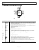
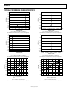
PIN CONFIGURATION AND FUNCTION DESCRIPTIONS
PIN 1
INDICATOR
1PS2/ADR5/D5
NOTES
1. EXPOSED PAD SHOULD BE SOLDERED TO GROUND.
2PS1/ADR4/D4
3PS0/ADR3/D3
4DVDD
5DGND
6ADR2/D2
7ADR1/D1
8ADR0/D0
24 RSET
23 AGND
22 AVDD
21 AGND
20 IOUT
19 IOUT
18 AGND
17 AVDD
9
SYNC
_
CLK
10
SER/PA
R
11
AGND
12
AVDD
13
REF
_
CLK
14
REF
_
CLK
15
A
GND
16
AVDD
32
ADR6/D6
31
ADR7/D7
30
SCLK(PCLK)
29
SDIO(W
R/R
D)
28
CS
27
IO_UPDATE
26
PWR_DW
N_CTL
25
MASTER_
RESET
TOP VIEW
(Not to Scale)
AD9913
07002-003
Figure 3. Pin Configuration
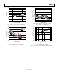
Table 3. Pin Function Descriptions
Pin No. Mnemonic I/O Description
1 PS2/ADR5/D5 I/O
Multipurpose pin: Profile Select Pin (PS2) in Direct Switch Mode, Parallel Port Address Line (ADR5), and
Data Line (D5) to program registers.
2 PS1/ADR4/D4 I/O
Multipurpose pin: Profile Select Pin (PS1) in Direct Switch Mode or Linear Sweeping Mode, Parallel Port
Address Line (ADR4), and Data Line (D4) to program registers.
3 PS0/ADR3/D3 I/O
Multipurpose pin: Profile Select Pin (PS0) in Direct Switch Mode or Linear Sweeping Mode, Parallel Port
Address Line (ADR3), and Data Line (D3) to program registers.
4 DVDD I Digital Power Supply (1.8 V).
5 DGND I Digital Ground.
6 ADR2/D2 I/O Parallel Port Address Line 2 and Data Line 2.
7 ADR1/D1 I/O Parallel Port Address Line 1and Data Line 1.
8 ADR0/D0 I/O Parallel Port Address Line 0 and Data Line 0.
9 SYNC_CLK O
Clock Out. The profile pins [PS0:PS2] and the IO_UPDATE pin (Pin 27) should be set up to the rising
edge of this signal to maintain constant pipe line delay through the device.
10
SER
/PAR
I Serial Port and Parallel Port Selection. Logic low = serial mode; logic high = parallel mode.
11, 15,
18, 21,
23
AGND I Analog Ground.
12, 16,
17, 22
AVDD I Analog Power Supply (1.8 V).
13 REF_CLK I Reference Clock Input. See the REF_CLK Overview section for more details.
14
REF_CLK
I Complementary Reference Clock Input. See the REF_CLK Overview section for more details.
19
IOUT
O Open Source DAC Complementary Output Source. Current mode. Connect through 50 Ω to AGND.
20 IOUT O Open Source DAC Output Source. Current mode. Connect through 50 Ω to AGND.
24 RSET I
Analog Reference. This pin programs the DAC output full-scale reference current. Attach a 4.64 kΩ
resistor to AGND.
25 MASTER_RESET I
Master Reset, Digital Input (Active High). This pin clears all memory elements and reprograms registers
to default values.