
Datasheet


AD9913
Rev. A | Page 5 of 32
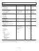
ABSOLUTE MAXIMUM RATINGS
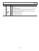
Table 2.
Parameter Rating
Maximum Junction Temperature 150°C
AVDD, DVDD 2 V
Digital Input Voltage −0.7 V to +2.2 V
Digital Output Current 5 mA
Storage Temperature –65°C to +150°C
Operating Temperature –40°C to +105°C
Lead Temperature (Soldering, 10 sec) 300°C
θ
JA
36.1°C/W
θ
JC
4.2°C/W
Stresses above those listed under Absolute Maximum Ratings
may cause permanent damage to the device. This is a stress
rating only and functional operation of the device at these or
any other conditions above those indicated in the operational
section of this specification is not implied. Exposure to absolute
maximum rating conditions for extended periods may affect
device reliability.
ESD CAUTION
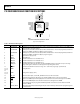
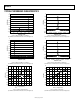
EQUIVALENT CIRCUITS
DIGITAL INPUTS
INPUT
DVDD_I/O
IOUT IOUT
DAC OUTPUTS
AVDD
A
VOID OVERDRIVING DIGITAL INPUTS.
FORWARD BIASING ESD DIODES MAY
C
OUPLE DIGITAL NOISE ONTO POWER
PINS.
MUST TERMINATE OUTPUTS TO AGND
FOR CURRENT FLOW. DO NOT EXCEED
THE OUTPUT VOLTAGE COMPLIANCE
RATING.
07002-002
Figure 2. Equivalent Input and Output Circuits