
Datasheet
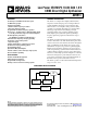


AD9913
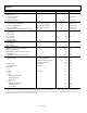
Rev. A | Page 4 of 32
Parameter Conditions/Comments Min Typ Max Unit
MISCELLANEOUS TIMING CHARACTERISTICS
Wake-Up Time
1
Fast Recovery Mode 1 SYSCLK cycles
2
Full Sleep Mode 60 s
Reset Pulse Width High 5 SYSCLK cycles
DATA LATENCY (PIPELINE DELAY)
Frequency, Phase-to-DAC Output Matched latency enabled 11 SYSCLK cycles
Frequency-to-DAC Output Matched latency disabled 11 SYSCLK cycles
Phase-to-DAC Output Matched latency disabled 10 SYSCLK cycles
Delta Tuning Word-to-DAC Output (Linear Sweep) 14 SYSCLK cycles
CMOS LOGIC INPUTS
Logic 1 Voltage 1.2 V
Logic 0 Voltage 0.4 V
Logic 1 Current −700 +700 nA
Logic 0 Current −700 +700 nA
Input Capacitance 3 pF
CMOS LOGIC OUTPUTS 1 mA load
Logic 1 Voltage 1.5 V
Logic 0 Voltage 0.125 V
POWER SUPPLY CURRENT
DVDD (1.8 V) Pin Current Consumption 46.5 mA
DAC_CLK_AVDD (1.8 V) 4.7 mA
DAC_AVDD (1.8 V) Pin Current Consumption 6.2 mA
PLL_AVDD (1.8 V) 1.8 mA
CLK_AVDD (1.8 V) Pin Current Consumption 4.3 mA
POWER CONSUMPTION
Single Tone Mode PLL enabled, CMOS input 50 66.5 mW
PLL disabled, differential input 57 70.5 mW
PLL enabled, XTAL input 52 68.5 mW
Modulus Mode PLL disabled 94.6 mW
Linear Sweep Mode PLL disabled 98.4 mW
Power-Down
Full 15 mW
Safe PLL enabled 44.8 mW
PLL Modes
VCO 1
Differential Input Mode 11 mW
CMOS Input Mode 7.5 mW
Crystal Mode 5.4 mW
VCO 2
Differential Input Mode 15 mW
CMOS Input Mode 11.5 mW
Crystal Mode 9.4 mW
1
Refer to the Power-Down Features section.
2
SYSCLK cycle refers to the actual clock frequency used on-chip by the DDS. If the reference clock multiplier is used to multiply the external reference clock frequency,
the SYSCLK frequency is the external frequency multiplied by the reference clock multiplication factor. If the reference clock multiplier and divider are not used, the
SYSCLK frequency is the same as the external reference clock frequency.