Datasheet
Manuals
Brands
ANALOG DEVICES Manuals
Data collecting ICs
Data acquisition IC - DA converter (DAC) TSSOP 28
11
12
13
14
15
16
17
18
19
20
REV. B
AD9764
–19–
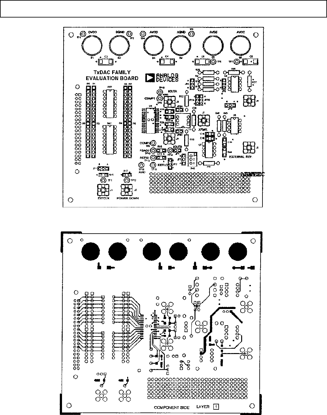
Figure 42.
Silkscreen Layer—Top
Figure 43.
Component Side PCB Layout (Layer 1)
1
...
...
17
18
19
20
21
...
22