
Datasheet


AD9549
Rev. D | Page 65 of 76
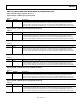
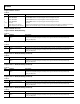
Register 0x0305—IRQ Mask (Continued)
Table 77.
Bits Bit Name Description
4 Frequency estimator done Trigger IRQ when the frequency estimator is done.
3 Phase unlock Trigger IRQ on falling edge of phase lock signal.
2 Phase lock Trigger IRQ on rising edge of phase lock signal.
1 Frequency unlock Trigger IRQ on falling edge of frequency lock signal.
0 Frequency lock Trigger IRQ on rising edge of frequency lock signal.
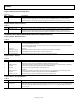
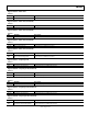
Register 0x0306—IRQ Mask (Continued)
Table 78.
Bits Bit Name Description
[7:6] Reserved Reserved.
5 REFA valid Trigger IRQ on rising edge of Reference A’s valid.
4 !REFA valid Trigger IRQ on falling edge of Reference A’s valid.
3 REFA LOR Trigger IRQ on rising edge of Reference A’s LOR.
2 !REFA LOR Trigger IRQ on falling edge of Reference A’s LOR.
1 REFA OOL Trigger IRQ on rising edge of Reference A’s OOL.
0 !REFA OOL Trigger IRQ on falling edge of Reference A’s OOL.
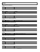
Register 0x0307—IRQ Mask (Continued)
Table 79.
Bits Bit Name Description
[7:6] Reserved Reserved.
5 REFB valid Trigger IRQ on rising edge of Reference B’s valid.
4 !REFB valid Trigger IRQ on falling edge of Reference B’s valid.
3 REFB LOR Trigger IRQ on rising edge of Reference B’s LOR.
2 !REFB LOR Trigger IRQ on falling edge of Reference B’s LOR.
1 REFB OOL Trigger IRQ on rising edge of Reference B’s OOL.
0 !REFB OOL Trigger IRQ on falling edge of Reference B’s OOL.
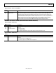
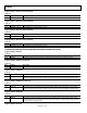
Register0x0308—S1 Pin Configuration
See the Status and Warnings section. The choice of input for a given pin must be all REFA or all REFB and not a combination of both.
Table 80.
Bits Bit Name Description
7 REF? Choose either REFA (0) or REFB (1) for use with Bits [4:6].
6 REF? LOR Select either REFA (0) or REFB (1) LOR signal for output on this pin.
5 REF? OOL Select either REFA (0) or REFB (1) OOL signal for output on this pin.
4 REF? not valid Select either REFA (0) or REFB (1). Not Valid signal for output on this pin.
3 Phase lock Select phase lock signal for output on this pin.
2 Frequency lock Select frequency lock signal for output on this pin.
1 Reserved Reserved.
0 IRQ Select IRQ signal for output on this pin.
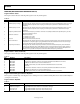
Register 0x0309—S2 Pin Configuration
Same as Register 0x0308, except applies to Pin S2. See Table 80.
Register 0x030A—S3 Pin Configuration
Same as Register 0x0308, except applies to Pin S3. See Table 80.
Register 0x030B—S4 Pin Configuration
Same as Register 0x0308, except applies to Pin S4. See Table 80.